- 您现在的位置:买卖IC网 > PDF目录1900 > ADV3002BSTZ-RL (Analog Devices Inc)IC SWITCH HDMI/DVI 4:1 80-LQFP PDF资料下载
参数资料
| 型号: | ADV3002BSTZ-RL |
| 厂商: | Analog Devices Inc |
| 文件页数: | 7/28页 |
| 文件大小: | 0K |
| 描述: | IC SWITCH HDMI/DVI 4:1 80-LQFP |
| 产品变化通告: | Marking Change 25/Mar/2009 |
| 标准包装: | 1,000 |
| 功能: | 开关 |
| 电路: | 1 x 4:1 |
| 电压电源: | 单电源 |
| 电压 - 电源,单路/双路(±): | 3 V ~ 3.6 V |
| 工作温度: | 0°C ~ 85°C |
| 安装类型: | 表面贴装 |
| 封装/外壳: | 80-LQFP |
| 供应商设备封装: | 80-LQFP(14x14) |
| 包装: | 带卷 (TR) |
第1页第2页第3页第4页第5页第6页当前第7页第8页第9页第10页第11页第12页第13页第14页第15页第16页第17页第18页第19页第20页第21页第22页第23页第24页第25页第26页第27页第28页
Data Sheet
ADV3002
Rev. B | Page 15 of 28
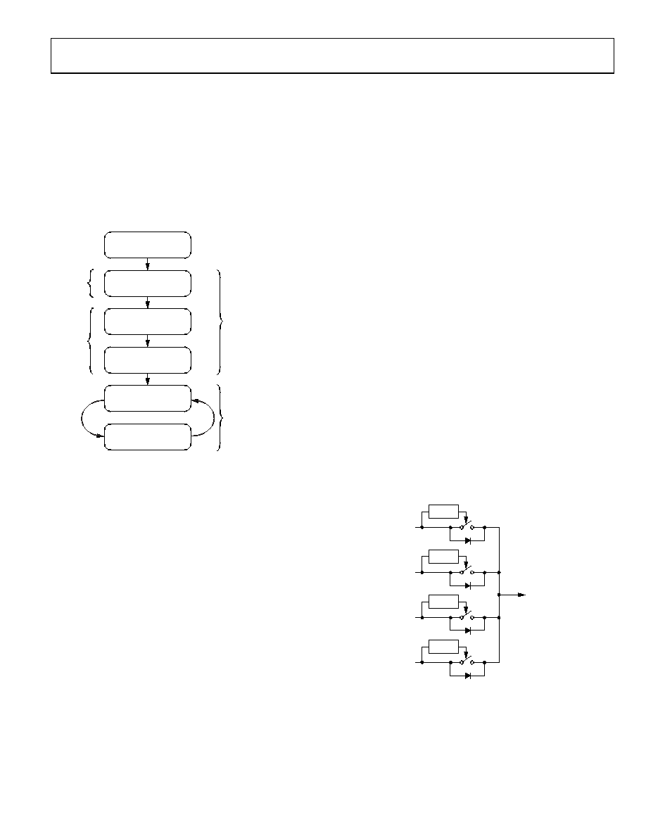
EDID Replication with External EEPROM
The ADV3002 has dedicated pins to interface to an external
EDID EEPROM: EDID_SDA and EDID_SCL. In the default
configuration, after the first hot plug event or system power-up,
the external EDID EEPROM into the on-chip SRAM. While the
EDID is being copied, the HPD signals for all four ports are held
low by the ADV3002. A flowchart of the start-up procedure is
shown in Figure 29. The entire start-up procedure takes less than
10 ms. The EDID replication feature can be disabled using the
EDID_ENABLE pin.
POWER-UP, RESET,
OR FIRST HOT PLUG
WAIT
FOR EDID POWER-UP
COPY EDID INFORMATION
TO ADV3002 SRAM
DETERMINE SPA
AND CHECKSUM
WAIT FOR EDID
REQUEST
RESPOND TO EDID
REQUEST
HPD ALL PORTS = LOW
HPD ALL PORTS = HIGH
<100s
<10ms
07905-
009
Figure 29. EDID Replication Start-Up Flowchart with External EEPROM
Writing to the EDID EEPROM
The EDID data can be written to the external EEPROM by
writing data via the I2C control interface or via the HDMI A
DDC inputs. In both cases, the EDID write procedure is as
follows:
1. Write Value 0x96 to the EDID EEPROM write protect
password register, Register 0x0F. The ADV3002 fixed part
address is required to write to this register.
2. Write the EDID data to the EEPROM fixed part address.
Data must be written one byte at a time.
3. Write Value 0x00 to the EDID EEPROM write protect
password register, Register 0x0F.
EDID Replication with External Microcontroller
The on-chip SRAM can be preloaded using an external micro-
controller. Prior to loading the SRAM, disable the I2C master by
writing 0x01 to the EDID replication mode register, Register 0x0E.
The microcontroller can then write EDID information into the
SRAM should be to the fixed part address of 0xA0. When the
EDID copy process is complete, enable the EDID replication
function by writing 0x00 to the EDID replication mode register
(Register 0x0E). The EDID_SDA and EDID_SCL pins are
unused when an external microcontroller is used to program
the SRAM. These pins can be tied either high or low through a
resistor, but should not be left floating.
Reset
Pullling the RESETB pin low initiates a restart of the EDID
replication procedure shown in Figure 29 when the local system
supply is on. If the local system supply is off, the RESETB pin
has no effect.
5 V COMBINER
The 5 V combiner circuit combines the four 5 V supplies from
the four HDMI sources and provides the necessary power to the
ADV3002 EDID replication circuit, the CEC buffer, as well as
the external EDID EEPROM, if applicable. The combiner circuit is
designed such that the current limits on each of the 5 V supplies
are not exceeded when the local system power is either on or off.
A simplified circuit diagram of the 5 V combiner is shown in
Figure 30. The combiner detects the presence of the voltage on
the 5 V pin (P5V_x) from the HDMI connectors and closes the
respective internal switch to connect the 5 V to AMUXVCC. If
the local system 3.3 V and 5 V supplies are available, then the
combiner opens all the switches.
P5V_A
P5V_B
P5V_C
P5V_D
AMUXVCC
07905-
010
DETECT
Figure 30. 5 V Combiner Simplified Circuit Diagram
相关PDF资料 |
PDF描述 |
|---|---|
| ADV3003ACPZ-R7 | IC EQUALZR HDMI/DVI TMDS 40LFCSP |
| ADV3200ASWZ | IC CROSSPOINT SWIT 32X32 176LQFP |
| ADV3203ASWZ | IC CROSSPOINT SWIT 32X16 176LQFP |
| ADV3205JSTZ | IC CROSSPOINT SWIT 16X16 100LQFP |
| ADV3220ACPZ-R7 | IC MULTIPLEXER 2:1 16LFCSP |
相关代理商/技术参数 |
参数描述 |
|---|---|
| ADV3002-EVALZ | 制造商:AD 制造商全称:Analog Devices 功能描述:4:1 HDMI/DVI Switch with Equalization, DDC/CEC Buffers and EDID Replication |
| ADV3002XSTZ | 功能描述:IC SWITCH HDMI/DVI 4:1 80LQFP 制造商:analog devices inc. 系列:- 包装:托盘 零件状态:上次购买时间 类型:视频开关 应用:HDTV,投影仪,机顶盒 安装类型:- 封装/外壳:- 供应商器件封装:- 标准包装:1 |
| ADV3002XSTZ-RL | 功能描述:IC SWITCH HDMI/DVI 4:1 80LQFP 制造商:analog devices inc. 系列:- 包装:带卷(TR) 零件状态:上次购买时间 类型:视频开关 应用:HDTV,投影仪,机顶盒 安装类型:- 封装/外壳:- 供应商器件封装:- 标准包装:1 |
| ADV3003 | 制造商:AD 制造商全称:Analog Devices 功能描述:HDMI/DVI TMDS Equalizer |
| ADV3003ACPZ | 功能描述:IC EQUALZR HDMI/DVI TMDS 40LFCSP RoHS:是 类别:集成电路 (IC) >> 接口 - 专用 系列:- 特色产品:NXP - I2C Interface 标准包装:1 系列:- 应用:2 通道 I²C 多路复用器 接口:I²C,SM 总线 电源电压:2.3 V ~ 5.5 V 封装/外壳:16-TSSOP(0.173",4.40mm 宽) 供应商设备封装:16-TSSOP 包装:剪切带 (CT) 安装类型:表面贴装 产品目录页面:825 (CN2011-ZH PDF) 其它名称:568-1854-1 |
发布紧急采购,3分钟左右您将得到回复。