- 您现在的位置:买卖IC网 > PDF目录1900 > ADV3002BSTZ-RL (Analog Devices Inc)IC SWITCH HDMI/DVI 4:1 80-LQFP PDF资料下载
参数资料
| 型号: | ADV3002BSTZ-RL |
| 厂商: | Analog Devices Inc |
| 文件页数: | 4/28页 |
| 文件大小: | 0K |
| 描述: | IC SWITCH HDMI/DVI 4:1 80-LQFP |
| 产品变化通告: | Marking Change 25/Mar/2009 |
| 标准包装: | 1,000 |
| 功能: | 开关 |
| 电路: | 1 x 4:1 |
| 电压电源: | 单电源 |
| 电压 - 电源,单路/双路(±): | 3 V ~ 3.6 V |
| 工作温度: | 0°C ~ 85°C |
| 安装类型: | 表面贴装 |
| 封装/外壳: | 80-LQFP |
| 供应商设备封装: | 80-LQFP(14x14) |
| 包装: | 带卷 (TR) |
第1页第2页第3页当前第4页第5页第6页第7页第8页第9页第10页第11页第12页第13页第14页第15页第16页第17页第18页第19页第20页第21页第22页第23页第24页第25页第26页第27页第28页
ADV3002
Data Sheet
Rev. B | Page 12 of 28
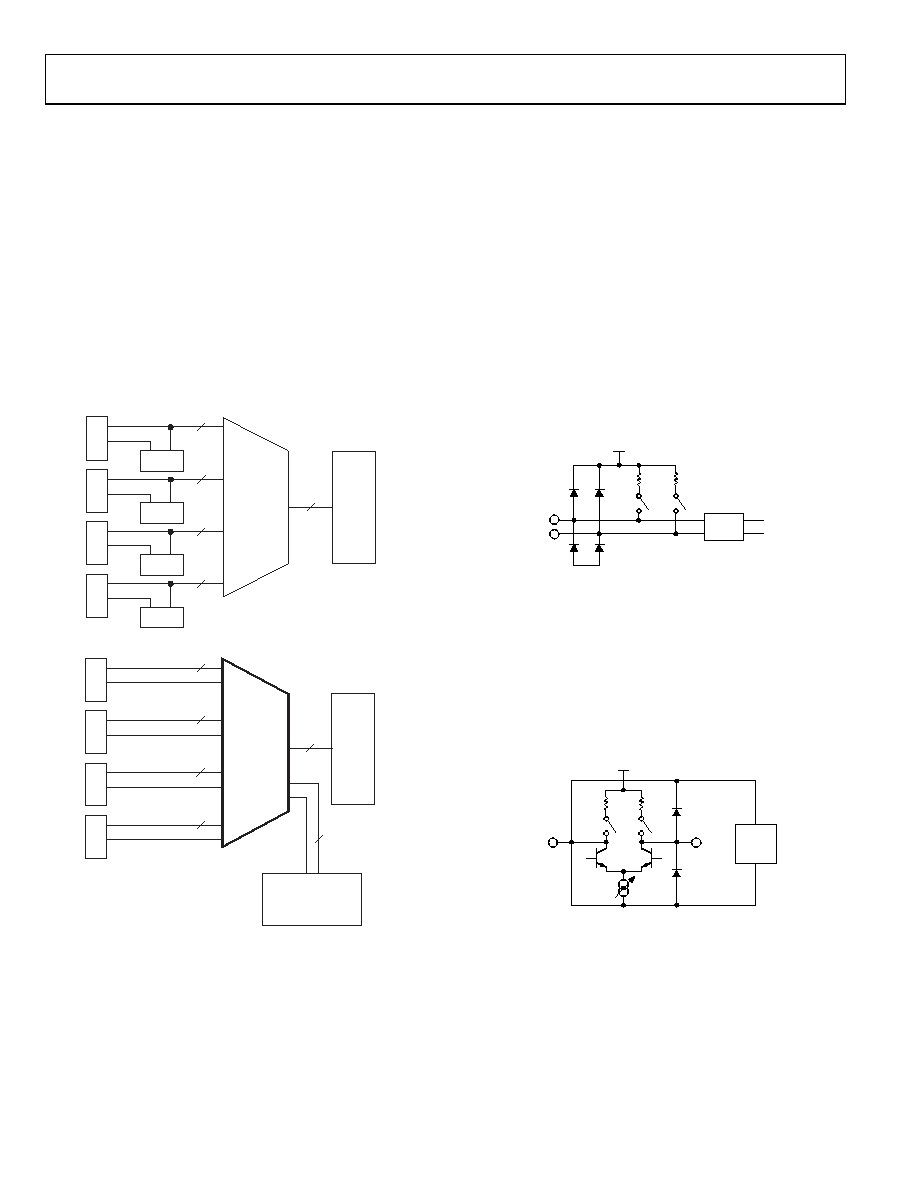
THEORY OF OPERATION
The primary function of the ADV3002 is to switch up to four
HDMI/DVI sources to one HDMI/DVI sink. Each HDMI/DVI
link consists of four differential, high speed channels and four
auxiliary single-ended, low speed signals. The high speed channels
include a data-word clock and three TMDS data channels running
at 10× the data-word clock frequency for data rates up to 2.25
Gbps. The four low speed control signals are the display data
channel (DDC) bus (SDA and SCL), the consumer electronics
control (CEC) line, and the hot plug detect (HPD) signal.
The ADV3002 also includes an integrated EDID SRAM,
eliminating the need for an external EDID EEPROM for each
HDMI connector. A typical HDMI multiplexer is shown in
Figure 23. The simplified implementation using the ADV3002
is shown in Figure 24.
HDMI
Rx
HDM
IA
DDC
5V
2
EDID A
HDM
IB
DDC
5V
2
EDID B
HDM
IC
DDC
5V
2
EDID C
HDM
ID
DDC
5V
2
EDID D
4:1
HDMI
MUX
07905-
003
Figure 23. Typical HDMI Multiplexer
HDMI
Rx
HDM
IA
DDC
5V
2
EXTERNAL
EDID EEPROM
OR SYSTEM
MICROCONTROLLER
HDM
IB
DDC
5V
AMUXVCC
2
HDM
IC
DDC
EDID DDC
5V
2
HDM
ID
DDC
5V
2
ADV3002
07905-
004
Figure 24. Simplified Implementation Using the ADV3002
TMDS INPUT CHANNELS
Each high speed input differential pair terminates to the 3.3 V
power supply through a pair of 50 on-chip resistors, as shown
in Figure 25. The state of the input terminations can be configured
automatically or programmed manually by setting the appropriate
bits in the TMDS input termination control register, as shown
The input equalizer can be manually configured to provide
two different levels of high frequency boost: 4 dB or 16 dB for
2.25 Gbps data. The equalizer (EQ) level defaults to 16 dB after
reset. No specific cable length is suggested for a particular
equalization setting because cable performance varies widely
between manufacturers; however, in general, the equalization of
the ADV3002 can be set to 16 dB without degrading the signal
integrity, even for short input cables.
50
CABLE
EQ
AVCC
AVEE
IN+
IN–
NOTES
1. IN+ REFERS TO IN_x_CLK+/IN_x_DATAx+ PINS.
2. IN– REFERS TO IN_x_CLK–/IN_x_DATAx– PINS.
07905-
005
Figure 25. High Speed Input Simplified Schematic
TMDS OUTPUT CHANNELS
Each high speed output differential pair is terminated to the 3.3 V
power supply through a pair of 50 on-chip resistors, as shown
in Figure 26. This termination is user-selectable; it can be
turned on or off by programming the TX_OTO bit of the TMDS
output control register, as shown in Table 10.
50
OUT+
OUT–
ESD
PROT.
AVCC
AVEE
NOTES
1. OUT+ REFERS TO OUT_CLK+ AND OUT_DATAx+ PINS.
2. OUT– REFERS TO OUT_CLK– AND OUT_DATAx– PINS.
DISABLE
IOUT
07905-
006
Figure 26. High Speed Output Simplified Schematic
The output termination resistors of the ADV3002 back
terminate the output TMDS transmission lines. These back
terminations, as recommended in the HDMI 1.4 specification,
act to absorb reflections from impedance discontinuities on the
output traces, improving the signal integrity of the output traces
and adding flexibility to how the output traces can be routed.
相关PDF资料 |
PDF描述 |
|---|---|
| ADV3003ACPZ-R7 | IC EQUALZR HDMI/DVI TMDS 40LFCSP |
| ADV3200ASWZ | IC CROSSPOINT SWIT 32X32 176LQFP |
| ADV3203ASWZ | IC CROSSPOINT SWIT 32X16 176LQFP |
| ADV3205JSTZ | IC CROSSPOINT SWIT 16X16 100LQFP |
| ADV3220ACPZ-R7 | IC MULTIPLEXER 2:1 16LFCSP |
相关代理商/技术参数 |
参数描述 |
|---|---|
| ADV3002-EVALZ | 制造商:AD 制造商全称:Analog Devices 功能描述:4:1 HDMI/DVI Switch with Equalization, DDC/CEC Buffers and EDID Replication |
| ADV3002XSTZ | 功能描述:IC SWITCH HDMI/DVI 4:1 80LQFP 制造商:analog devices inc. 系列:- 包装:托盘 零件状态:上次购买时间 类型:视频开关 应用:HDTV,投影仪,机顶盒 安装类型:- 封装/外壳:- 供应商器件封装:- 标准包装:1 |
| ADV3002XSTZ-RL | 功能描述:IC SWITCH HDMI/DVI 4:1 80LQFP 制造商:analog devices inc. 系列:- 包装:带卷(TR) 零件状态:上次购买时间 类型:视频开关 应用:HDTV,投影仪,机顶盒 安装类型:- 封装/外壳:- 供应商器件封装:- 标准包装:1 |
| ADV3003 | 制造商:AD 制造商全称:Analog Devices 功能描述:HDMI/DVI TMDS Equalizer |
| ADV3003ACPZ | 功能描述:IC EQUALZR HDMI/DVI TMDS 40LFCSP RoHS:是 类别:集成电路 (IC) >> 接口 - 专用 系列:- 特色产品:NXP - I2C Interface 标准包装:1 系列:- 应用:2 通道 I²C 多路复用器 接口:I²C,SM 总线 电源电压:2.3 V ~ 5.5 V 封装/外壳:16-TSSOP(0.173",4.40mm 宽) 供应商设备封装:16-TSSOP 包装:剪切带 (CT) 安装类型:表面贴装 产品目录页面:825 (CN2011-ZH PDF) 其它名称:568-1854-1 |
发布紧急采购,3分钟左右您将得到回复。