- 您现在的位置:买卖IC网 > PDF目录1900 > ADV3002BSTZ-RL (Analog Devices Inc)IC SWITCH HDMI/DVI 4:1 80-LQFP PDF资料下载
参数资料
| 型号: | ADV3002BSTZ-RL |
| 厂商: | Analog Devices Inc |
| 文件页数: | 18/28页 |
| 文件大小: | 0K |
| 描述: | IC SWITCH HDMI/DVI 4:1 80-LQFP |
| 产品变化通告: | Marking Change 25/Mar/2009 |
| 标准包装: | 1,000 |
| 功能: | 开关 |
| 电路: | 1 x 4:1 |
| 电压电源: | 单电源 |
| 电压 - 电源,单路/双路(±): | 3 V ~ 3.6 V |
| 工作温度: | 0°C ~ 85°C |
| 安装类型: | 表面贴装 |
| 封装/外壳: | 80-LQFP |
| 供应商设备封装: | 80-LQFP(14x14) |
| 包装: | 带卷 (TR) |
第1页第2页第3页第4页第5页第6页第7页第8页第9页第10页第11页第12页第13页第14页第15页第16页第17页当前第18页第19页第20页第21页第22页第23页第24页第25页第26页第27页第28页
Data Sheet
ADV3002
Rev. B | Page 25 of 28
Any one group of four TMDS traces (Input A, Input B, Input C,
Input D, or the output) should have closely matched trace
lengths to minimize interpair skew. Severe interpair skew can
cause the data on the four different channels of a group to arrive
out of alignment with one another. A good practice is to match
the trace lengths for a given group of four channels to within
0.05 inches on FR4 material.
Minimizing intrapair and interpair skew becomes increasingly
important as data rates increase. Any introduced skew consti-
tutes a correspondingly larger fraction of a bit period at higher
data rates.
Though the ADV3002 features input equalization and output
preemphasis, minimizing the length of the TMDS traces is needed
to reduce overall system signal degradation. Commonly used
PCB material, such as FR4, is lossy at high frequencies; therefore,
long traces on the circuit board increase signal attenuation,
resulting in decreased signal swing and increased jitter through
intersymbol interference (ISI).
Controlling the Characteristic Impedance of a TMDS
Differential Pair
The characteristic impedance of a differential pair depends on
a number of variables, including the trace width, the distance
between the two traces, the height of the dielectric material
between the trace and the reference plane below it, and the
dielectric constant of the PCB binder material. To a lesser
extent, the characteristic impedance also depends upon the
trace thickness and the presence of solder mask. Many
combinations can produce the correct characteristic impedance.
Generally, working with the PCB fabricator is required to obtain
a set of parameters to produce the desired results.
One consideration is how to guarantee a differential pair with
a differential impedance of 100 over the entire length of the
trace. One technique to accomplish this is to change the width
of the traces in a differential pair based on how closely one trace
is coupled to the other. When the two traces of a differential pair
are close and strongly coupled, they should have a width that
produces a100 differential impedance. When the traces split
apart to go into a connector, for example, and are no longer so
strongly coupled, the width of the traces need to be increased to
yield a differential impedance of 100 in the new configuration.
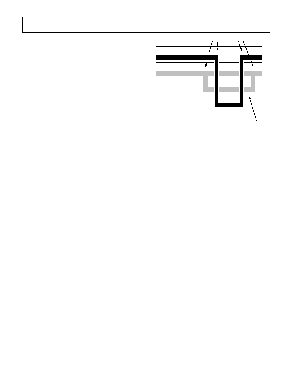
Ground Current Return
In some applications, it can be necessary to invert the output
pin order of the ADV3002. This requires a designer to route the
TMDS traces on multiple layers of the PCB. When routing dif-
ferential pairs on multiple layers, it is necessary to also reroute
the corresponding reference plane to provide one continuous
ground current return path for the differential signals. Standard
plated through-hole vias are acceptable for both the TMDS
traces and the reference plane. An example of this is illustrated
PCB DIELECTRIC
SILKSCREEN
PCB DIELECTRIC
LAYER 2: GND (REFERENCE PLANE)
LAYER 4: SIGNAL (MICROSTRIP)
THROUGH-HOLE VIAS
LAYER 1: SIGNAL (MICROSTRIP)
KEEP REFERENCE PLANE
ADJACENT TO SIGNAL ON ALL
LAYERS TO PROVIDE CONTINUOUS
GROUND CURRENT RETURN PATH.
LAYER 3: PWR
(REFERENCE PLANE)
07905-
019
Figure 39. Example Routing of Reference Plane
TMDS Terminations
The ADV3002 provides internal 50 single-ended terminations
for all of its high speed inputs and outputs. It is not necessary to
include external termination resistors for the TMDS differential
pairs on the PCB.
The output termination resistors of the ADV3002 back terminate
the output TMDS transmission lines. These back terminations
act to absorb reflections from impedance discontinuities on the
output traces, improving the signal integrity of the output traces
and adding flexibility to how the output traces can be routed.
For example, interlayer vias can be used to route the ADV3002
TMDS outputs on multiple layers of the PCB without severely
degrading the quality of the output signal.
Auxiliary Control Signals
There are four single-ended control signals associated with each
source or sink in an HDMI/DVI application. These are hot plug
detect (HPD), consumer electronics control (CEC), and two
display data channel (DDC) lines. The two signals on the DDC
bus are SDA and SCL (serial data and serial clock, respectively).
The DDC and CEC signals are buffered and switched through
the ADV3002, and the HPD signal is pulsed low by the ADV3002.
These signals do not need to be routed with the same strict
considerations as the high speed TMDS signals.
In general, it is sufficient to route each auxiliary signal as a
single-ended trace. These signals are not sensitive to impedance
discontinuities, do not require a reference plane, and can be
routed on multiple layers of the PCB. However, it is best to
follow strict layout practices whenever possible to prevent the
PCB design from affecting the overall application. The specific
routing of the HPD, CEC, and DDC lines depends upon the
application in which the ADV3002 is being used.
相关PDF资料 |
PDF描述 |
|---|---|
| ADV3003ACPZ-R7 | IC EQUALZR HDMI/DVI TMDS 40LFCSP |
| ADV3200ASWZ | IC CROSSPOINT SWIT 32X32 176LQFP |
| ADV3203ASWZ | IC CROSSPOINT SWIT 32X16 176LQFP |
| ADV3205JSTZ | IC CROSSPOINT SWIT 16X16 100LQFP |
| ADV3220ACPZ-R7 | IC MULTIPLEXER 2:1 16LFCSP |
相关代理商/技术参数 |
参数描述 |
|---|---|
| ADV3002-EVALZ | 制造商:AD 制造商全称:Analog Devices 功能描述:4:1 HDMI/DVI Switch with Equalization, DDC/CEC Buffers and EDID Replication |
| ADV3002XSTZ | 功能描述:IC SWITCH HDMI/DVI 4:1 80LQFP 制造商:analog devices inc. 系列:- 包装:托盘 零件状态:上次购买时间 类型:视频开关 应用:HDTV,投影仪,机顶盒 安装类型:- 封装/外壳:- 供应商器件封装:- 标准包装:1 |
| ADV3002XSTZ-RL | 功能描述:IC SWITCH HDMI/DVI 4:1 80LQFP 制造商:analog devices inc. 系列:- 包装:带卷(TR) 零件状态:上次购买时间 类型:视频开关 应用:HDTV,投影仪,机顶盒 安装类型:- 封装/外壳:- 供应商器件封装:- 标准包装:1 |
| ADV3003 | 制造商:AD 制造商全称:Analog Devices 功能描述:HDMI/DVI TMDS Equalizer |
| ADV3003ACPZ | 功能描述:IC EQUALZR HDMI/DVI TMDS 40LFCSP RoHS:是 类别:集成电路 (IC) >> 接口 - 专用 系列:- 特色产品:NXP - I2C Interface 标准包装:1 系列:- 应用:2 通道 I²C 多路复用器 接口:I²C,SM 总线 电源电压:2.3 V ~ 5.5 V 封装/外壳:16-TSSOP(0.173",4.40mm 宽) 供应商设备封装:16-TSSOP 包装:剪切带 (CT) 安装类型:表面贴装 产品目录页面:825 (CN2011-ZH PDF) 其它名称:568-1854-1 |
发布紧急采购,3分钟左右您将得到回复。