参数资料
| 型号: | AGLE600V5-FGG484I |
| 厂商: | Microsemi SoC |
| 文件页数: | 33/166页 |
| 文件大小: | 0K |
| 描述: | IC FPGA 1KB FLASH 600K 484-FBGA |
| 标准包装: | 60 |
| 系列: | IGLOOe |
| 逻辑元件/单元数: | 13824 |
| RAM 位总计: | 110592 |
| 输入/输出数: | 270 |
| 门数: | 600000 |
| 电源电压: | 1.425 V ~ 1.575 V |
| 安装类型: | 表面贴装 |
| 工作温度: | -40°C ~ 85°C |
| 封装/外壳: | 484-BGA |
| 供应商设备封装: | 484-FPBGA(23x23) |
第1页第2页第3页第4页第5页第6页第7页第8页第9页第10页第11页第12页第13页第14页第15页第16页第17页第18页第19页第20页第21页第22页第23页第24页第25页第26页第27页第28页第29页第30页第31页第32页当前第33页第34页第35页第36页第37页第38页第39页第40页第41页第42页第43页第44页第45页第46页第47页第48页第49页第50页第51页第52页第53页第54页第55页第56页第57页第58页第59页第60页第61页第62页第63页第64页第65页第66页第67页第68页第69页第70页第71页第72页第73页第74页第75页第76页第77页第78页第79页第80页第81页第82页第83页第84页第85页第86页第87页第88页第89页第90页第91页第92页第93页第94页第95页第96页第97页第98页第99页第100页第101页第102页第103页第104页第105页第106页第107页第108页第109页第110页第111页第112页第113页第114页第115页第116页第117页第118页第119页第120页第121页第122页第123页第124页第125页第126页第127页第128页第129页第130页第131页第132页第133页第134页第135页第136页第137页第138页第139页第140页第141页第142页第143页第144页第145页第146页第147页第148页第149页第150页第151页第152页第153页第154页第155页第156页第157页第158页第159页第160页第161页第162页第163页第164页第165页第166页
Pin Descriptions and Packaging
3-4
Revision 13
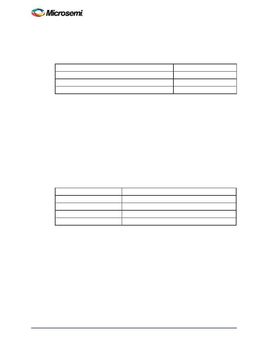
Table 3-1 shows the Flash*Freeze pin location on the available packages. The Flash*Freeze pin location
is independent of device (except for a PQ208 package), allowing migration to larger or smaller IGLOO
devices while maintaining the same pin location on the board. Refer to the "Flash*Freeze Technology
and Low Power Modes" chapter of the IGLOOe FPGA Fabric User’s Guide for more information on I/O
states during Flash*Freeze mode.
JTAG Pins
Low power flash devices have a separate bank for the dedicated JTAG pins. The JTAG pins can be run
at any voltage from 1.5 V to 3.3 V (nominal). VCC must also be powered for the JTAG state machine to
operate, even if the device is in bypass mode; VJTAG alone is insufficient. Both VJTAG and VCC to the
part must be supplied to allow JTAG signals to transition the device. Isolating the JTAG power supply in a
separate I/O bank gives greater flexibility in supply selection and simplifies power supply and PCB
design. If the JTAG interface is neither used nor planned for use, the VJTAG pin together with the TRST
pin could be tied to GND.
TCK
Test Clock
Test clock input for JTAG boundary scan, ISP, and UJTAG. The TCK pin does not have an internal pull-
up/-down resistor. If JTAG is not used, Microsemi recommends tying off TCK to GND through a resistor
placed close to the FPGA pin. This prevents JTAG operation in case TMS enters an undesired state.
Note that to operate at all VJTAG voltages, 500
to 1 k will satisfy the requirements. Refer to Table 3-2
for more information.
Table 3-1 Flash*Freeze Pin Locations for IGLOOe Devices
Package
Flash*Freeze Pin
FG256
T3
FG484
W6
FG896
AH4
Table 3-2 Recommended Tie-Off Values for the TCK and TRST Pins
VJTAG
Tie-Off Resistance 1,2
VJTAG at 3.3 V
200
to 1 k
VJTAG at 2.5 V
200
to 1 k
VJTAG at 1.8 V
500
to 1 k
VJTAG at 1.5 V
500
to 1 k
Notes:
1. The TCK pin can be pulled-up or pulled-down.
2. The TRST pin is pulled-down.
3. Equivalent parallel resistance if more than one device is on the JTAG chain
相关PDF资料 |
PDF描述 |
|---|---|
| EMC55DRST-S273 | CONN EDGECARD 110PS DIP .100 SLD |
| RSA50DRMD-S664 | CONN EDGECARD 100POS .125 SQ WW |
| A42MX24-2PQG160I | IC FPGA MX SGL CHIP 36K 160-PQFP |
| EPF10K50VBC356-3N | IC FLEX 10KV FPGA 50K 356-BGA |
| EPF10K50VBC356-3 | IC FLEX 10KV FPGA 50K 356-BGA |
相关代理商/技术参数 |
参数描述 |
|---|---|
| AGLE600V5-FGG896 | 制造商:ACTEL 制造商全称:Actel Corporation 功能描述:IGLOOe Low-Power Flash FPGAs with Flash Freeze Technology |
| AGLE600V5-FGG896ES | 制造商:ACTEL 制造商全称:Actel Corporation 功能描述:IGLOOe Low-Power Flash FPGAs with Flash Freeze Technology |
| AGLE600V5-FGG896I | 制造商:ACTEL 制造商全称:Actel Corporation 功能描述:IGLOOe Low-Power Flash FPGAs with Flash Freeze Technology |
| AGLE600V5-FGG896PP | 制造商:ACTEL 制造商全称:Actel Corporation 功能描述:IGLOOe Low-Power Flash FPGAs with Flash Freeze Technology |
| AGL-ICICLE-KIT | 功能描述:KIT EVAL FOR IGOO ICICLE RoHS:是 类别:编程器,开发系统 >> 通用嵌入式开发板和套件(MCU、DSP、FPGA、CPLD等) 系列:IGLOO 产品培训模块:Blackfin® Processor Core Architecture Overview Blackfin® Device Drivers Blackfin® Optimizations for Performance and Power Consumption Blackfin® System Services 特色产品:Blackfin? BF50x Series Processors 标准包装:1 系列:Blackfin® 类型:DSP 适用于相关产品:ADSP-BF548 所含物品:板,软件,4x4 键盘,光学拨轮,QVGA 触摸屏 LCD 和 40G 硬盘 配用:ADZS-BFBLUET-EZEXT-ND - EZ-EXTENDER DAUGHTERBOARDADZS-BFLLCD-EZEXT-ND - BOARD EXT LANDSCAP LCD INTERFACE 相关产品:ADSP-BF542BBCZ-4A-ND - IC DSP 16BIT 400MHZ 400CSBGAADSP-BF544MBBCZ-5M-ND - IC DSP 16BIT 533MHZ MDDR 400CBGAADSP-BF542MBBCZ-5M-ND - IC DSP 16BIT 533MHZ MDDR 400CBGAADSP-BF542KBCZ-6A-ND - IC DSP 16BIT 600MHZ 400CSBGAADSP-BF547MBBCZ-5M-ND - IC DSP 16BIT 533MHZ MDDR 400CBGAADSP-BF548BBCZ-5A-ND - IC DSP 16BIT 533MHZ 400CSBGAADSP-BF547BBCZ-5A-ND - IC DSP 16BIT 533MHZ 400CSBGAADSP-BF544BBCZ-5A-ND - IC DSP 16BIT 533MHZ 400CSBGAADSP-BF542BBCZ-5A-ND - IC DSP 16BIT 533MHZ 400CSBGA |
发布紧急采购,3分钟左右您将得到回复。