- 您现在的位置:买卖IC网 > PDF目录166215 > AM29F800BB-70SD (SPANSION LLC) Flash Memory IC; Memory Size:8Mbit; Package/Case:44-SOIC; Leaded Process Compatible:Yes; Peak Reflow Compatible (260 C):Yes; Supply Voltage Max:5V; Access Time, Tacc:70ns; Series:AM29 RoHS Compliant: Yes PDF资料下载
参数资料
| 型号: | AM29F800BB-70SD |
| 厂商: | SPANSION LLC |
| 元件分类: | PROM |
| 英文描述: | Flash Memory IC; Memory Size:8Mbit; Package/Case:44-SOIC; Leaded Process Compatible:Yes; Peak Reflow Compatible (260 C):Yes; Supply Voltage Max:5V; Access Time, Tacc:70ns; Series:AM29 RoHS Compliant: Yes |
| 中文描述: | 512K X 16 FLASH 5V PROM, 70 ns, PDSO44 |
| 封装: | LEAD FREE, MO-180AA, SOP-44 |
| 文件页数: | 9/45页 |
| 文件大小: | 1402K |
| 代理商: | AM29F800BB-70SD |
第1页第2页第3页第4页第5页第6页第7页第8页当前第9页第10页第11页第12页第13页第14页第15页第16页第17页第18页第19页第20页第21页第22页第23页第24页第25页第26页第27页第28页第29页第30页第31页第32页第33页第34页第35页第36页第37页第38页第39页第40页第41页第42页第43页第44页第45页
March 3, 2009 21504E6
Am29F800B
15
D A TA SH EE T
Autoselect Command Sequence
The autoselect command sequence allows the host
system to access the manufacturer and devices codes,
and determine whether or not a sector is protected.
The Command Definitions table shows the address
and data requirements. This method is an alternative to
that shown in the Autoselect Codes (High Voltage
Method) table, which is intended for PROM program-
mers and requires VID on address bit A9.
The autoselect command sequence is initiated by
writing two unlock cycles, followed by the autoselect
command. The device then enters the autoselect
mode, and the system may read at any address any
number of times, without initiating another command
sequence.
A read cycle at address XX00h or retrieves the manu-
facturer code. A read cycle at address XX01h in word
mode (or 02h in byte mode) returns the device code.
A read cycle containing a sector address (SA) and the
address 02h in word mode (or 04h in byte mode) re-
turns 01h if that sector is protected, or 00h if it is un-
protected. Refer to the Sector Address tables for valid
sector addresses.
The system must write the reset command to exit the
autoselect mode and return to reading array data.
Word/Byte Program Command Sequence
The system may program the device by byte or word,
on depending on the state of the BYTE# pin. Program-
ming is a four-bus-cycle operation. The program com-
mand sequence is initiated by writing two unlock write
cycles, followed by the program set-up command. The
program address and data are written next, which in
turn initiate the Embedded Program algorithm. The
system is not required to provide further controls or tim-
ings. The device automatically provides internally gen-
erated program pulses and verify the programmed cell
margin. The Command Definitions take shows the ad-
dress and data requirements for the byte program com-
mand sequence.
When the Embedded Program algorithm is complete,
the device then returns to reading array data and ad-
dresses are no longer latched. The system can deter-
mine the status of the program operation by using DQ7,
DQ6, or RY/BY#. See “Write Operation Status” for in-
formation on these status bits.
Any commands written to the device during the Em-
bedded Program Algorithm are ignored. Note that a
hardware reset immediately terminates the program-
ming operation. The program command sequence
should be reinitiated once the device has reset to read-
ing array data, to ensure data integrity.
Programming is allowed in any sequence and across
sector boundaries. A bit cannot be programmed
from a “0” back to a “1”. Attempting to do so may halt
the operation and set DQ5 to “1”, or cause the Data#
Polling algorithm to indicate the operation was suc-
cessful. However, a succeeding read will show that the
data is still “0”. Only erase operations can convert a “0”
to a “1”.
Note: See the appropriate Command Definitions table for
program command sequence.
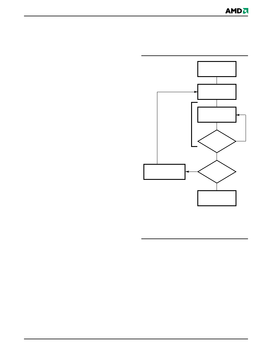
Figure 2.
Program Operation
Chip Erase Command Sequence
Chip erase is a six-bus-cycle operation. The chip erase
command sequence is initiated by writing two unlock
cycles, followed by a set-up command. Two additional
unlock write cycles are then followed by the chip erase
command, which in turn invokes the Embedded Erase
algorithm. The device does not require the system to
preprogram prior to erase. The Embedded Erase algo-
rithm automatically preprograms and verifies the entire
memory for an all zero data pattern prior to electrical
erase. The system is not required to provide any con-
trols or timings during these operations. The Command
Definitions table shows the address and data require-
ments for the chip erase command sequence.
START
Write Program
Command Sequence
Data Poll
from System
Verify Data?
No
Yes
Last Address?
No
Yes
Programming
Completed
Increment Address
Embedded
Program
algorithm
in progress
相关PDF资料 |
PDF描述 |
|---|---|
| AM29F800BB-90ED | FLASH BOTTOM BLOCK 8MB, SMD, 29F800; Memory type:Bottom Block; Memory size:8Mbit; Memory configuration:1Mx8 or 512Kx16; Time, access:90ns; Voltage, Memory Vcc:5V; Case style:TSOP; Temperature, operating range:0(degree C) to RoHS Compliant: Yes |
| AM29F800BB-90EF | Flash Memory IC; Leaded Process Compatible:Yes; Memory Size:8Mbit; Package/Case:48-TSOP; Peak Reflow Compatible (260 C):Yes; Supply Voltage Max:5V; Access Time, Tacc:90ns; Series:AM29 RoHS Compliant: Yes |
| AM29F800BB-90SC | Flash Memory IC; Access Time, Tacc:90ns; Package/Case:44-SO; Leaded Process Compatible:No; Memory Configuration:512K x 16 / 1M x 8; Memory Size:8Mbit; Peak Reflow Compatible (260 C):No; Supply Voltage Max:5.5V RoHS Compliant: No |
| AM29F800BB-90SD | Flash Memory IC; Memory Size:8Mbit; Package/Case:44-SOIC; Leaded Process Compatible:Yes; Peak Reflow Compatible (260 C):Yes; Supply Voltage Max:5V; Access Time, Tacc:90ns; Series:AM29 RoHS Compliant: Yes |
| AM29F800BB-90SF | Flash Memory IC; Leaded Process Compatible:Yes; Memory Size:8Mbit; Package/Case:44-SOIC; Peak Reflow Compatible (260 C):Yes; Supply Voltage Max:5V; Access Time, Tacc:90ns; Series:AM29 RoHS Compliant: Yes |
相关代理商/技术参数 |
参数描述 |
|---|---|
| AM29F800BB-70SD | 制造商:Spansion 功能描述:FLASH MEMORY IC |
| AM29F800BB-70SE | 制造商:Spansion 功能描述:NOR Flash Parallel 5V 8Mbit 1M/512K x 8bit/16bit 70ns 44-Pin SO |
| AM29F800BB-70SF | 功能描述:闪存 8M (1MX8/512KX16) Parallel NOR Fl 5V RoHS:否 制造商:ON Semiconductor 数据总线宽度:1 bit 存储类型:Flash 存储容量:2 MB 结构:256 K x 8 定时类型: 接口类型:SPI 访问时间: 电源电压-最大:3.6 V 电源电压-最小:2.3 V 最大工作电流:15 mA 工作温度:- 40 C to + 85 C 安装风格:SMD/SMT 封装 / 箱体: 封装:Reel |
| AM29F800BB-70SI | 制造商:Spansion 功能描述:8M CMOS FLASH 5V |
| AM29F800BB-90EC | 制造商:Spansion 功能描述:8M CMOS FLASH 5V |
发布紧急采购,3分钟左右您将得到回复。