- 您现在的位置:买卖IC网 > PDF目录295065 > AM79C965KCW (ADVANCED MICRO DEVICES INC) 3 CHANNEL(S), LOCAL AREA NETWORK CONTROLLER, PQFP16 PDF资料下载
参数资料
| 型号: | AM79C965KCW |
| 厂商: | ADVANCED MICRO DEVICES INC |
| 元件分类: | 微控制器/微处理器 |
| 英文描述: | 3 CHANNEL(S), LOCAL AREA NETWORK CONTROLLER, PQFP16 |
| 封装: | PLASTIC, QFP-160 |
| 文件页数: | 92/220页 |
| 文件大小: | 1197K |
| 代理商: | AM79C965KCW |
第1页第2页第3页第4页第5页第6页第7页第8页第9页第10页第11页第12页第13页第14页第15页第16页第17页第18页第19页第20页第21页第22页第23页第24页第25页第26页第27页第28页第29页第30页第31页第32页第33页第34页第35页第36页第37页第38页第39页第40页第41页第42页第43页第44页第45页第46页第47页第48页第49页第50页第51页第52页第53页第54页第55页第56页第57页第58页第59页第60页第61页第62页第63页第64页第65页第66页第67页第68页第69页第70页第71页第72页第73页第74页第75页第76页第77页第78页第79页第80页第81页第82页第83页第84页第85页第86页第87页第88页第89页第90页第91页当前第92页第93页第94页第95页第96页第97页第98页第99页第100页第101页第102页第103页第104页第105页第106页第107页第108页第109页第110页第111页第112页第113页第114页第115页第116页第117页第118页第119页第120页第121页第122页第123页第124页第125页第126页第127页第128页第129页第130页第131页第132页第133页第134页第135页第136页第137页第138页第139页第140页第141页第142页第143页第144页第145页第146页第147页第148页第149页第150页第151页第152页第153页第154页第155页第156页第157页第158页第159页第160页第161页第162页第163页第164页第165页第166页第167页第168页第169页第170页第171页第172页第173页第174页第175页第176页第177页第178页第179页第180页第181页第182页第183页第184页第185页第186页第187页第188页第189页第190页第191页第192页第193页第194页第195页第196页第197页第198页第199页第200页第201页第202页第203页第204页第205页第206页第207页第208页第209页第210页第211页第212页第213页第214页第215页第216页第217页第218页第219页第220页
P R E L I M I N A R Y
AMD
181
Am79C965
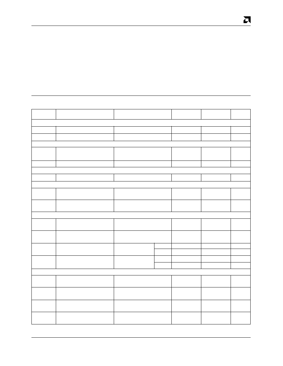
ABSOLUTE MAXIMUM RATINGS
Storage Temperature
–65
°C to +150°C
. . . . . . . . . . .
Ambient Temperature
Under Bias
–65
°C to +125°C
. . . . . . . . . . . . . . . . . . .
Supply Voltage to AVss
or DVSS (AVDD, DVDD)
–0.3 V to +6.0 V
. . . . . . . . . . .
Stresses above those listed under Absolute Maximum Rat-
ings may cause permanent device failure. Functionality at or
above these limits is not implied. Exposure to Absolute Maxi-
mum Ratings for extended periods may affect device reliabil-
ity. Programming conditions may differ.
OPERATING RANGES
Commercial (C) Devices
Temperature (TA)0
°C to +70°C
. . . . . . . . . . . . . . . . .
Supply Voltages
(AVDD, DVDD)5 V
±5%
. . . . . . . . . . . . . . . . . . . . . . . .
All inputs within the range:
AVSS – 0.5 V
≤ Vin ≤
. . . . .
AVDD + 0.5 V, or
DVSS – 0.5 V
≤ Vin ≤
DVDD + 0.5 V
Operating ranges define those limits between which the func-
tionality of the device is guaranteed.
DC CHARACTERISTICS over COMMERCIAL operating ranges unless otherwise
specified
Parameter
Symbol
Parameter Description
Test Conditions
Min
Max
Unit
Digital Input Voltage
VIL
Input LOW Voltage
0.8
V
VIH
Input HIGH Voltage
2.0
V
Digital Ouput Voltage
VOL
Output LOW Voltage
IOL1 = 8 mA, IOL2 = 4 mA
0.45
V
(Notes 1 and 5)
VOH
Output HIGH Voltage (Note 2)
IOH = –4 mA (Note 5)
2.4
V
Digital Input Leakage Current
IIX
Input Leakage Current (Note 3)
VDD = 5 V, VIN = 0 V
–10
10
A
Digital Ouput Leakage Current
IOZL
Output Low Leakage
VOUT = 0 V
–10
A
Current (Note 4)
IOZH
Output High Leakage
VOUT = VDD
10
A
Current (Note 4)
Crystal Input
VILX
XTAL1 Input LOW
VIN = External Clock
–0.5
0.8
V
Threshold Voltage
VILHX
XTAL1 Input HIGH
VIN = External Clock
VDD–0.8
VDD + 0.5
V
Threshold Voltage
Attachment Unit Interface
IIAXD
Input Current at DI+
–1 V < VIN < AVDD +0.5 V
–500
+500
A
and DI–
IIAXC
Input Current at
–1 V < VIN < AVDD +0.5 V
–500
+500
A
CI+ and CI–
VAOD
Differential Output Voltage
RL = 78
630
1200
mV
|(DO+)–(DO–)|
VAODOFF
Transmit Differential Output
RL = 78
(Note 9)
–40
+40
mV
Idle Voltage
Active
Sleep
Active
Sleep
IILX
XTAL1 Input LOW Current
IIHX
XTAL1 Input HIGH Current
VIN = 0 V
VIN = VDD
0
–10
+10
A
120
400
A
–120
0
相关PDF资料 |
PDF描述 |
|---|---|
| AM80A-024L-120F18 | 1-OUTPUT 240 W DC-DC REG PWR SUPPLY MODULE |
| AJ80A-024L-033F50 | 1-OUTPUT 240 W DC-DC REG PWR SUPPLY MODULE |
| AM93LC66S | 4096-bits Serial Electrically Erasable PROM |
| AM93LC66SA | 4096-bits Serial Electrically Erasable PROM |
| AM93LC66VN | 4096-bits Serial Electrically Erasable PROM |
相关代理商/技术参数 |
参数描述 |
|---|---|
| AM79C970 | 制造商:AMD 制造商全称:Advanced Micro Devices 功能描述:PCnetTM-PCI Single-Chip Ethernet Controller for PCI Local Bus |
| AM79C970A | 制造商:AMD 制造商全称:Advanced Micro Devices 功能描述:PCnet-PCI II Single-Chip Full-Duplex Ethernet Controller for PCI Local Bus Product |
| AM79C970AKC | 制造商:AMD 制造商全称:Advanced Micro Devices 功能描述:PCnet-PCI II Single-Chip Full-Duplex Ethernet Controller for PCI Local Bus Product |
| AM79C970AKC\\W | 制造商:Rochester Electronics LLC 功能描述:- Bulk 制造商:Advanced Micro Devices 功能描述: |
发布紧急采购,3分钟左右您将得到回复。