- 您现在的位置:买卖IC网 > PDF目录166232 > AS7C25512FT32A-85BIN (ALLIANCE SEMICONDUCTOR CORP) 512K X 32 STANDARD SRAM, 8.5 ns, PBGA165 PDF资料下载
参数资料
| 型号: | AS7C25512FT32A-85BIN |
| 厂商: | ALLIANCE SEMICONDUCTOR CORP |
| 元件分类: | SRAM |
| 英文描述: | 512K X 32 STANDARD SRAM, 8.5 ns, PBGA165 |
| 封装: | LEAD FREE, BGA-165 |
| 文件页数: | 20/24页 |
| 文件大小: | 574K |
| 代理商: | AS7C25512FT32A-85BIN |
4/12/04, v. 1.0
Alliance Semiconductor
5 of 24
AS7C25512FT32A
AS7C25512FT36A
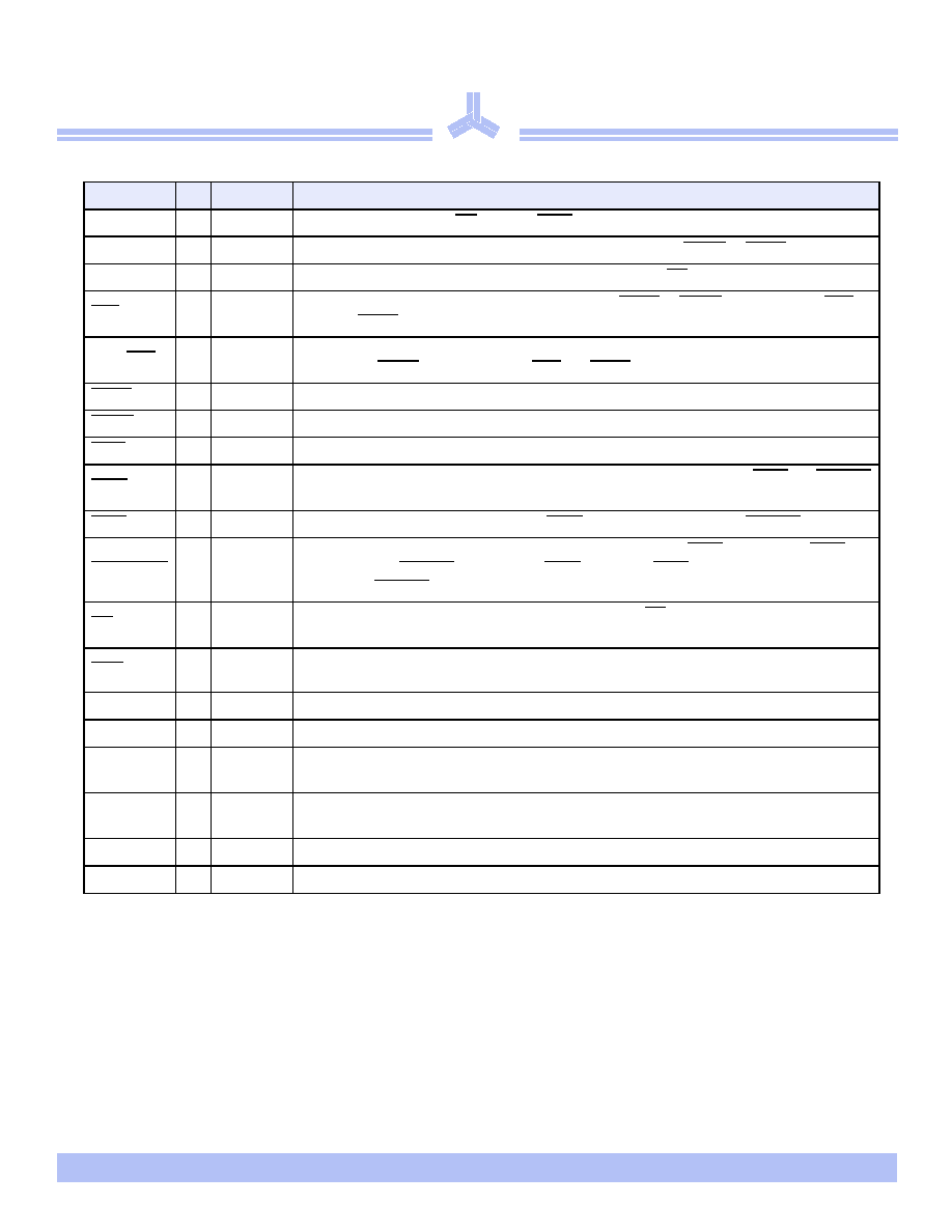
Signal descriptions
Pin
I/O Properties Description
CLK
I
CLOCK
Clock. All inputs except OE, ZZ, and LBO are synchronous to this clock.
A,A0,A1
I
SYNC
Address. Sampled when all chip enables are active and when ADSC or ADSP are asserted.
DQ[a,b,c,d]
I/O
SYNC
Data. Driven as output when the chip is enabled and when OE is active.
CE0
ISYNC
Master chip enable. Sampled on clock edges when ADSP or ADSC is active. When CE0 is
inactive, ADSP is blocked. Refer to the “Synchronous truth table” for more information.
CE1, CE2
ISYNC
Synchronous chip enables, active HIGH, and active LOW, respectively. Sampled on clock
edges when ADSC is active or when CE0 and ADSP are active.
ADSP
I
SYNC
Address strobe processor. Asserted LOW to load a new address or to enter standby mode.
ADSC
I
SYNC
Address strobe controller. Asserted LOW to load a new address or to enter standby mode.
ADV
I
SYNC
Advance. Asserted LOW to continue burst read/write.
GWE
ISYNC
Global write enable. Asserted LOW to write all 32/36 bits. When HIGH, BWE and BW[a:d]
control write enable.
BWE
I
SYNC
Byte write enable. Asserted LOW with GWE HIGH to enable effect of BW[a:d] inputs.
BW[a,b,c,d]
ISYNC
Write enables. Used to control write of individual bytes when GWE is HIGH and BWE is
LOW. If any of BW[a:d] is active with GWE HIGH and BWE LOW, the cycle is a write
cycle. If all BW[a:d] are inactive, the cycle is a read cycle.
OE
I
ASYNC
Asynchronous output enable. I/O pins are driven when OE is active and chip is in read
mode.
LBO
ISTATIC
Selects Burst mode. When tied to VDD or left floating, device follows interleaved Burst order. When
driven LOW, device follows linear Burst order. This signal is internally pulled High.
TDO
O
SYNC
Serial data-out to the JTAG circuit. Delivers data on the negative edge of TCK (BGA only).
TDI
I
SYNC
Serial data-in to the JTAG circuit. Sampled on the rising edge of TCK (BGA only).
TMS
I
SYNC
This pin controls the Test Access Port state machine. Sampled on the rising edge of TCK
(BGA only).
TCK
I
Test Clock
Test Clock. All inputs are sampled on the rising edge of TCK. All outputs are driven from
the falling edge of TCK.
ZZ
I
ASYNC
Snooze. Places device in low power mode; data is retained. Connect to GND if unused.
NC
-
no connects
相关PDF资料 |
PDF描述 |
|---|---|
| AS7C25512NTD32A-166TQI | 512K X 32 ZBT SRAM, 3.5 ns, PQFP100 |
| AS7C3256K18Z-3.5TQC | 256K X 18 STANDARD SRAM, 3.5 ns, PQFP100 |
| AS7C33512NTD18A-166BC | 512K X 18 ZBT SRAM, 9 ns, PBGA119 |
| AS7C3364FT36B-65TQCN | 64K X 36 STANDARD SRAM, 6.5 ns, PQFP100 |
| AS7C3364FT36B-80TQC | 64K X 36 STANDARD SRAM, 8 ns, PQFP100 |
相关代理商/技术参数 |
参数描述 |
|---|---|
| AS7C25512FT32A-85TQC | 制造商:ALSC 制造商全称:Alliance Semiconductor Corporation 功能描述:2.5V 512K x 32/36 flowthrough burst synchronous SRAM |
| AS7C25512FT32A-85TQCN | 制造商:ALSC 制造商全称:Alliance Semiconductor Corporation 功能描述:2.5V 512K x 32/36 flowthrough burst synchronous SRAM |
| AS7C25512FT32A-85TQI | 制造商:ALSC 制造商全称:Alliance Semiconductor Corporation 功能描述:2.5V 512K x 32/36 flowthrough burst synchronous SRAM |
| AS7C25512FT32A-85TQIN | 制造商:ALSC 制造商全称:Alliance Semiconductor Corporation 功能描述:2.5V 512K x 32/36 flowthrough burst synchronous SRAM |
| AS7C25512FT36A-10TQC | 制造商:ALSC 制造商全称:Alliance Semiconductor Corporation 功能描述:2.5V 512K x 32/36 flowthrough burst synchronous SRAM |
发布紧急采购,3分钟左右您将得到回复。