- 您现在的位置:买卖IC网 > PDF目录166232 > AS7C25512FT32A-85BIN (ALLIANCE SEMICONDUCTOR CORP) 512K X 32 STANDARD SRAM, 8.5 ns, PBGA165 PDF资料下载
参数资料
| 型号: | AS7C25512FT32A-85BIN |
| 厂商: | ALLIANCE SEMICONDUCTOR CORP |
| 元件分类: | SRAM |
| 英文描述: | 512K X 32 STANDARD SRAM, 8.5 ns, PBGA165 |
| 封装: | LEAD FREE, BGA-165 |
| 文件页数: | 3/24页 |
| 文件大小: | 574K |
| 代理商: | AS7C25512FT32A-85BIN |
4/12/04, v. 1.0
Alliance Semiconductor
11 of 24
AS7C25512FT32A
AS7C25512FT36A
IEEE 1149.1 serial boundary scan (JTAG)
The SRAM incorporates a serial boundary scan test access port (TAP). The port operates in accordance with IEEE Standard 1149.1-1990 but
does not have the set of functions required for full 1149.1 compliance. The inclusion of these functions would place an added delay in the
critical speed path of the SRAM. The TAP controller functionality does not conflict with the operation of other devices using 1149.1 fully
compliant TAPs. It uses JEDEC-standard 2.5V I/O logic levels.
The SRAM contains a TAP controller, instruction register, boundary scan register, bypass register, and ID register.
Disabling the JTAG feature
If the JTAG function is not being implemented, TCK should be tied to VSS, TMS and TDI can be left unconnected. At power-up, the device
will come up in a reset state which will not interfere with the operation of the device. TDO should be left unconnected.
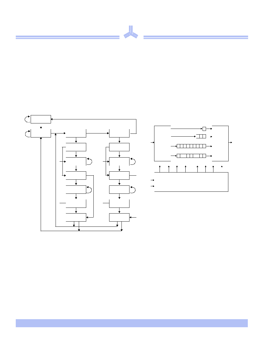
TAP controller state diagram
TAP controller block diagram
Test access port (TAP)
Test clock (TCK)
The test clock is used with only the TAP controller. All inputs are captured on the rising edge of TCK. All outputs are driven from the falling
edge of TCK.
Test mode select (TMS)
The TAP controller receives commands from TMS input. It is sampled on the rising edge of TCK. You can leave this pin/ball unconnected if
the TAP is not used. The pin/ball is pulled up internally, resulting in a logic high level.
UPDATE-IR
CAPTURE-IR
SHIFT-IR
EXIT1-IR
PAUSE-IR
EXIT2-IR
SELECT
IR-SCAN
UPDATE-DR
CAPTURE-DR
SHIFT-DR
EXIT1-DR
PAUSE-DR
EXIT2-DR
RUN-TEST/
IDLE
TEST-LOGIC
RESET
SELECT
DR-SCAN
0
1
0
00
0
11
1
11
1
Note: The 0 or 1 next to each state represents the value of TMS at the rising edge of TCK.
Selection
Circuitry
Selection
Circuitry
31 30 29
0
1
2
.
Boundary Scan Register1
Identification Register
Bypass Register
Instruction Register
x0
1
2
0
1
2
0
.. . . .
TDI
TMS
TCK
TDO
TAP Controller
1 x = 53 for the x18 configuration, x = 72 for the x36 configuration.
相关PDF资料 |
PDF描述 |
|---|---|
| AS7C25512NTD32A-166TQI | 512K X 32 ZBT SRAM, 3.5 ns, PQFP100 |
| AS7C3256K18Z-3.5TQC | 256K X 18 STANDARD SRAM, 3.5 ns, PQFP100 |
| AS7C33512NTD18A-166BC | 512K X 18 ZBT SRAM, 9 ns, PBGA119 |
| AS7C3364FT36B-65TQCN | 64K X 36 STANDARD SRAM, 6.5 ns, PQFP100 |
| AS7C3364FT36B-80TQC | 64K X 36 STANDARD SRAM, 8 ns, PQFP100 |
相关代理商/技术参数 |
参数描述 |
|---|---|
| AS7C25512FT32A-85TQC | 制造商:ALSC 制造商全称:Alliance Semiconductor Corporation 功能描述:2.5V 512K x 32/36 flowthrough burst synchronous SRAM |
| AS7C25512FT32A-85TQCN | 制造商:ALSC 制造商全称:Alliance Semiconductor Corporation 功能描述:2.5V 512K x 32/36 flowthrough burst synchronous SRAM |
| AS7C25512FT32A-85TQI | 制造商:ALSC 制造商全称:Alliance Semiconductor Corporation 功能描述:2.5V 512K x 32/36 flowthrough burst synchronous SRAM |
| AS7C25512FT32A-85TQIN | 制造商:ALSC 制造商全称:Alliance Semiconductor Corporation 功能描述:2.5V 512K x 32/36 flowthrough burst synchronous SRAM |
| AS7C25512FT36A-10TQC | 制造商:ALSC 制造商全称:Alliance Semiconductor Corporation 功能描述:2.5V 512K x 32/36 flowthrough burst synchronous SRAM |
发布紧急采购,3分钟左右您将得到回复。