参数资料
| 型号: | AT89C51SND2C-7FTUL |
| 厂商: | Atmel |
| 文件页数: | 160/160页 |
| 文件大小: | 0K |
| 描述: | IC 8051 MCU FLASH 64K MP3 100BGA |
| 标准包装: | 260 |
| 系列: | 89C |
| 核心处理器: | 8051 |
| 芯体尺寸: | 8-位 |
| 速度: | 40MHz |
| 连通性: | I²C,IDE/ATAPI,MMC,SPI,UART/USART,USB |
| 外围设备: | 音频,I²S,MP3,PCM,POR,WDT |
| 输入/输出数: | 32 |
| 程序存储器容量: | 64KB(64K x 8) |
| 程序存储器类型: | 闪存 |
| RAM 容量: | 2.25K x 8 |
| 电压 - 电源 (Vcc/Vdd): | 2.7 V ~ 3.3 V |
| 振荡器型: | 内部 |
| 工作温度: | -40°C ~ 85°C |
| 封装/外壳: | 100-TFBGA |
| 包装: | 托盘 |
| 其它名称: | AT89C51SND2C7FTUL |
第1页第2页第3页第4页第5页第6页第7页第8页第9页第10页第11页第12页第13页第14页第15页第16页第17页第18页第19页第20页第21页第22页第23页第24页第25页第26页第27页第28页第29页第30页第31页第32页第33页第34页第35页第36页第37页第38页第39页第40页第41页第42页第43页第44页第45页第46页第47页第48页第49页第50页第51页第52页第53页第54页第55页第56页第57页第58页第59页第60页第61页第62页第63页第64页第65页第66页第67页第68页第69页第70页第71页第72页第73页第74页第75页第76页第77页第78页第79页第80页第81页第82页第83页第84页第85页第86页第87页第88页第89页第90页第91页第92页第93页第94页第95页第96页第97页第98页第99页第100页第101页第102页第103页第104页第105页第106页第107页第108页第109页第110页第111页第112页第113页第114页第115页第116页第117页第118页第119页第120页第121页第122页第123页第124页第125页第126页第127页第128页第129页第130页第131页第132页第133页第134页第135页第136页第137页第138页第139页第140页第141页第142页第143页第144页第145页第146页第147页第148页第149页第150页第151页第152页第153页第154页第155页第156页第157页第158页第159页当前第160页
9
4341H–MP3–10/07
AT8xC51SND2C/MP3B
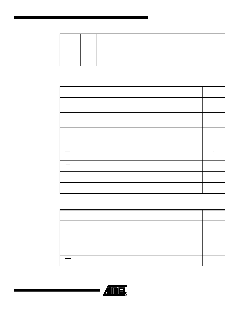
Table 4-11.
A/D Converter Signal Description (AT8XSND2CMP3B only)
Table 4-12.
External Access Signal Description
Note:
1. For ROM/Flash/ROMless Dice product versions only.
Table 4-13.
System Signal Description
Signal
Name
Type
Description
Alternate
Function
AIN1:0
I
A/D Analog Inputs
-
ADCREFP
I
Analog Positive Voltage Reference Input
-
ADCREFN
I
Analog Negative Voltage Reference Input
-
Signal
Name
Type
Description
Alternate
Function
A15:8
I/O
Address Lines
Upper address lines for the external bus.
Multiplexed higher address and data lines for the IDE interface.
P2.7:0
AD7:0
I/O
Address/Data Lines
Multiplexed lower address and data lines for the external memory or the IDE
interface.
P0.7:0
ALE
O
Address Latch Enable Output
ALE signals the start of an external bus cycle and indicates that valid address
information is available on lines A7:0. An external latch is used to demultiplex
the address from address/data bus.
-
ISP
I/O
ISP Enable Input (AT89C51SND2C Only)
This signal must be held to GND through a pull-down resistor at the falling
reset to force execution of the internal bootloader.
-
RD
O
Read Signal
Read signal asserted during external data memory read operation.
P3.7
WR
O
Write Signal
Write signal asserted during external data memory write operation.
P3.6
EA(1)
I
External Access Enable: EA must be externally held low to enable the device
to fetch code from external program memory locations 0000H to FFFFH (RD).
-
Signal
Name
Type
Description
Alternate
Function
RST
I
Reset Input
Holding this pin high for 64 oscillator periods while the oscillator is running
resets the device. The Port pins are driven to their reset conditions when a
voltage lower than V
IL is applied, whether or not the oscillator is running.
This pin has an internal pull-down resistor which allows the device to be reset
by connecting a capacitor between this pin and V
DD.
Asserting RST when the chip is in Idle mode or Power-Down mode returns the
chip to normal operation.
-
TST
I
Test Input
Test mode entry signal. This pin must be set to V
DD.
-
相关PDF资料 |
PDF描述 |
|---|---|
| AT89C52-24PI | IC MICRO CTRL 24MHZ 40DIP |
| AT89C55WD-24AU | IC 8051 MCU FLASH 20K 44TQFP |
| AT89EB5114-TGSIL | IC 8051 MCU FLASH 4K 20SOIC |
| AT89LP214-20PU | MCU 8051 2K FLASH 20MHZ 14-PDIP |
| AT89LP216-20SU | MCU 8051 2K FLASH 20MHZ 16-SOIC |
相关代理商/技术参数 |
参数描述 |
|---|---|
| AT89C51-W | 功能描述:8位微控制器 -MCU Microcontroller RoHS:否 制造商:Silicon Labs 核心:8051 处理器系列:C8051F39x 数据总线宽度:8 bit 最大时钟频率:50 MHz 程序存储器大小:16 KB 数据 RAM 大小:1 KB 片上 ADC:Yes 工作电源电压:1.8 V to 3.6 V 工作温度范围:- 40 C to + 105 C 封装 / 箱体:QFN-20 安装风格:SMD/SMT |
| AT89C52 | 制造商:ATMEL 制造商全称:ATMEL Corporation 功能描述:8-Bit Microcontroller with 8K Bytes Flash |
| AT89C52_00 | 制造商:ATMEL 制造商全称:ATMEL Corporation 功能描述:8-bit Microcontroller with 8K Bytes Flash |
| AT89C52_99 | 制造商:ATMEL 制造商全称:ATMEL Corporation 功能描述:8-bit Microcontroller with 8K Bytes Flash |
| AT89C52-12AA | 制造商:ATMEL 制造商全称:ATMEL Corporation 功能描述:8-Bit Microcontroller with 8K Bytes Flash |
发布紧急采购,3分钟左右您将得到回复。