- 您现在的位置:买卖IC网 > PDF目录166632 > BU-65743F3-200 (DATA DEVICE CORP) 2 CHANNEL(S), 1M bps, MIL-STD-1553 CONTROLLER, CQFP80 PDF资料下载
参数资料
| 型号: | BU-65743F3-200 |
| 厂商: | DATA DEVICE CORP |
| 元件分类: | 微控制器/微处理器 |
| 英文描述: | 2 CHANNEL(S), 1M bps, MIL-STD-1553 CONTROLLER, CQFP80 |
| 封装: | 0.880 INCH, CERAMIC, QFP-80 |
| 文件页数: | 51/75页 |
| 文件大小: | 532K |
| 代理商: | BU-65743F3-200 |
第1页第2页第3页第4页第5页第6页第7页第8页第9页第10页第11页第12页第13页第14页第15页第16页第17页第18页第19页第20页第21页第22页第23页第24页第25页第26页第27页第28页第29页第30页第31页第32页第33页第34页第35页第36页第37页第38页第39页第40页第41页第42页第43页第44页第45页第46页第47页第48页第49页第50页当前第51页第52页第53页第54页第55页第56页第57页第58页第59页第60页第61页第62页第63页第64页第65页第66页第67页第68页第69页第70页第71页第72页第73页第74页第75页
55
Data Device Corporation
www.ddc-web.com
BU-65743/65843/65863/65864
D-06/04-0
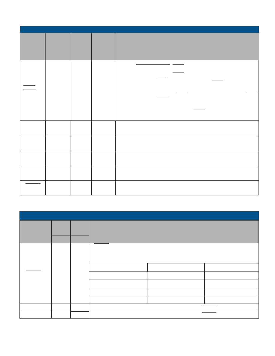
INCMD (O)/
MCRST (O)
19
In-command or Mode Code Reset. The function of this pin is controlled by bit 0 of Configuration
Register #7, MODE CODE RESET / INCMD SELECT.
If this register bit is logic "0" (default), INCMD will be active on this pin. For BC, RT, or Selective
Message Monitor modes, INCMD is asserted low whenever a message is being processed by
the PCI Mini-ACE Mark3/Micro-ACE TE. In Word Monitor mode, INCMD will be asserted low for
as long as the monitor is online.
For RT mode, if MODE CODE RESET/INCMD SELECT is programmed to logic "1", MCRST
will be active. In this case, MCRST will be asserted low for two clock cycles following receipt of
a Reset remote terminal mode command.
In BC or Monitor modes, if MODE CODE RESET/INCMD SELECT is logic "1", this signal is
inoperative; i.e., in this case, it will always output a value of logic "1".
E8
TABLE 74. MISCELLANEOUS SIGNALS
DESCRIPTION
BALL
5V
PIN
C9
BALL
3V
SIGNAL NAME
TAG_CLK (I)
23
Input (5V tolerant) for optional external tag clock. No connection needed if internal tag clock is
used. Maximum TAG_CLK frequency is 1/44th of the 1553_CLK input.
D18
F14
SLEEP_IN (I)
14
Sleep input for both 3.3V transceivers. SLEEP_IN = 1 puts the 3.3V transceivers in sleep mode
(receiver and transmitter disabled).
--
R4
1553_CLK (I)
78
20 MHz, 16 MHz, 12 MHz, or 10 MHz clock input.
D8
B7
TX_INH A/B
(I)
18
Transmitter inhibit input (5V tolerant) for the Channel A and Channel B MIL-STD-1553 transmit-
ters. For normal operation, this input should be connected to logic "0". To force a shutdown of
Channel A and Channel B, a value of logic "1" should be applied to the TX_INH input.
F10
F8
MSTCLR
(RST#) (I)
25
Master Clear. Negative true Reset input, normally asserted low following power turn-on. This
input conforms to PCI RST# convention.
B11
R18
RTBOOT (I)
F7
If RTBOOT is connected to Logic "0" the PCI Micro ACE TE will initialize in RT mode with the Busy sta-
tus word bit set following power turn on. Received data will not be stored because the “BUSY RECEIVE
TRANSFER DISABLE” bit will also be set following power turn on. In addition, CLK_SEL_0 and
CLK_SEL_1 are enabled and they select the divider for the 1553 clock circuitry:
TABLE 75. MISCELLANEOUS SIGNALS, BGA ONLY
SIGNAL NAME
DESCRIPTION
BALL
3V XCVR
C12
BALL
5V XCVR
CLK_SEL1
CLK_SEL0
1553 CLOCK FREQUENCY
0
10 MHz
0
1
20 MHz
1
0
12 MHz
1
16 MHz
1553 CLOCK SELECT 0, ACTIVE ONLY WHEN RTBOOT = 0
CLK_SEL_0 (I)
L14
M18
1553 CLOCK SELECT 1, ACTIVE ONLY WHEN RTBOOT = 0
CLK_SEL_1 (I)
E14
B15
相关PDF资料 |
PDF描述 |
|---|---|
| BU-65863F3-220 | 2 CHANNEL(S), 1M bps, MIL-STD-1553 CONTROLLER, CQFP80 |
| BU-65843B3-E02 | 2 CHANNEL(S), 1M bps, MIL-STD-1553 CONTROLLER, PBGA324 |
| BU-65863B8-E02 | 2 CHANNEL(S), 1M bps, MIL-STD-1553 CONTROLLER, PBGA324 |
| BU-65843B8-E02 | 2 CHANNEL(S), 1M bps, MIL-STD-1553 CONTROLLER, PBGA324 |
| BU1003 | POWER TRANSISTOR |
相关代理商/技术参数 |
参数描述 |
|---|---|
| BU6574FV | 制造商:ROHM 制造商全称:Rohm 功能描述:Silicon monolithic integrated circuit |
| BU6574FV-E2 | 功能描述:IC ANALOG FRONT END SSOP20 RoHS:是 类别:集成电路 (IC) >> 数据采集 - 模拟前端 (AFE) 系列:- 产品培训模块:Lead (SnPb) Finish for COTS Obsolescence Mitigation Program 标准包装:2,500 系列:- 位数:- 通道数:2 功率(瓦特):- 电压 - 电源,模拟:3 V ~ 3.6 V 电压 - 电源,数字:3 V ~ 3.6 V 封装/外壳:32-VFQFN 裸露焊盘 供应商设备封装:32-QFN(5x5) 包装:带卷 (TR) |
| BU6577FV | 制造商:ROHM 制造商全称:Rohm 功能描述:Silicon monolithic integrated circuit |
| BU6577FV-E2 | 制造商:ROHM Semiconductor 功能描述:ANALOG FRONT END - Tape and Reel |
| BU6581KV | 制造商:未知厂家 制造商全称:未知厂家 功能描述:コミュニケーションLSI |
发布紧急采购,3分钟左右您将得到回复。