- 您现在的位置:买卖IC网 > PDF目录298892 > BX80525U533512E (INTEL CORP) 32-BIT, 533 MHz, MICROPROCESSOR, XMA PDF资料下载
参数资料
| 型号: | BX80525U533512E |
| 厂商: | INTEL CORP |
| 元件分类: | 微控制器/微处理器 |
| 英文描述: | 32-BIT, 533 MHz, MICROPROCESSOR, XMA |
| 文件页数: | 11/94页 |
| 文件大小: | 898K |
| 代理商: | BX80525U533512E |
第1页第2页第3页第4页第5页第6页第7页第8页第9页第10页当前第11页第12页第13页第14页第15页第16页第17页第18页第19页第20页第21页第22页第23页第24页第25页第26页第27页第28页第29页第30页第31页第32页第33页第34页第35页第36页第37页第38页第39页第40页第41页第42页第43页第44页第45页第46页第47页第48页第49页第50页第51页第52页第53页第54页第55页第56页第57页第58页第59页第60页第61页第62页第63页第64页第65页第66页第67页第68页第69页第70页第71页第72页第73页第74页第75页第76页第77页第78页第79页第80页第81页第82页第83页第84页第85页第86页第87页第88页第89页第90页第91页第92页第93页第94页
Pentium
III Processor at 450 MHz, 500 MHz, 533B MHz, 550 MHz, 600/600B MHz
Datasheet
19
The CMOS, Clock, APIC, and TAP inputs can each be driven from ground to 2.5 V. The CMOS,
APIC, and TAP outputs are open drain and should be pulled high to 2.5 V. This ensures not only
correct operation for current Pentium III processors, but compatibility with future Pentium III
processors as well.
The groups and the signals contained within each group are shown in Table 4. Refer to Section 7.0
for a description of these signals.
NOTES:
1. The BR0# pin is the only BREQ# signal that is bidirectional. The internal BREQ# signals are mapped onto BR# pins
after the agent ID is determined. See Section 7.0 for more information.
2. See Section 7.0 for information on the PWRGOOD signal.
3. See Section 7.0 for information on the SLP# signal.
4. See Section 7.0 for information on the THERMTRIP# signal.
5. These signals are specified for 2.5 V operation.
6. VCC
CORE is the power supply for the processor core.
VCC
L2
is the power supply for the L2 cache component core logic.
VID[4:0] is described in Section 2.6.
VTT is used to terminate the system bus and generate VREF on the processor substrate.
VSS is system ground.
TESTHI should be connected to 2.5 V with a 100 k
resistor.
VCC
5 is not connected to the Pentium
III processor core. This supply is used for the test equipment and tools.
SLOTOCC# is described in Section 7.0.
BSEL[1:0] is described in Section 2.8.2 and Section 7.0.
EMI pins are described in Section 7.0.
THERMDP, THERMDN are described in Section 7.0.
2.8.1
Asynchronous vs. Synchronous for System Bus Signals
All AGTL+ signals are synchronous to BCLK. All of the CMOS, Clock, APIC, and TAP signals
can be applied asynchronously to BCLK.
All APIC signals are synchronous to PICCLK. All TAP signals are synchronous to TCK.
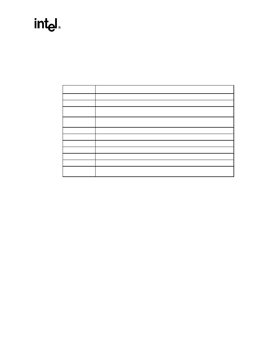
Table 4.
System Bus Signal Groups
Group Name
Signals
AGTL+ Input
BPRI#, BR1#, DEFER#, RESET#, RS[2:0]#, RSP#, TRDY#
AGTL+ Output
PRDY#
AGTL+ I/O
A[35:3]#, ADS#, AERR#, AP[1:0]#, BERR#, BINIT#, BNR#, BP[3:2]#, BPM[1:0]#, BR0#1,
D[63:0]#, DBSY#, DEP[7:0]#, DRDY#, HIT#, HITM#, LOCK#, REQ[4:0]#, RP#
CMOS Input5
A20M#, FLUSH#, IGNNE#, INIT#, LINT0/INTR, LINT1/NMI, PREQ#, PWRGOOD2, SMI#,
SLP#3, STPCLK#
CMOS Output5
FERR#, IERR#, THERMTRIP#4
System Bus Clock
BCLK
APIC Clock
PICCLK
APIC I/O5
PICD[1:0]
TAP Input5
TCK, TDI, TMS, TRST#
TAP Output5
TDO
Power/Other6
VCC
CORE, VCCL2, VCC5, VID[4:0], VTT, VSS, SLOTOCC#, THERMDP, THERMDN,
BSEL[1:0], EMI, TESTHI, Reserved
相关PDF资料 |
PDF描述 |
|---|---|
| BX80525U550512E | 32-BIT, 550 MHz, MICROPROCESSOR, XMA |
| BX80525U450512E | 32-BIT, 450 MHz, MICROPROCESSOR, XMA |
| BX80526F500256E | 32-BIT, 500 MHz, MICROPROCESSOR, PPGA370 |
| BX80526F650256E | 32-BIT, 650 MHz, MICROPROCESSOR, PPGA370 |
| BX80526F750256E | 32-BIT, 750 MHz, MICROPROCESSOR, PPGA370 |
相关代理商/技术参数 |
参数描述 |
|---|---|
| BX80525U550256E | 制造商:未知厂家 制造商全称:未知厂家 功能描述:Microprocessor |
| BX80525U600256E | 制造商:未知厂家 制造商全称:未知厂家 功能描述:Microprocessor |
| BX80525U600256EB | 制造商:未知厂家 制造商全称:未知厂家 功能描述:Microprocessor |
| BX80525U650256 | 制造商:未知厂家 制造商全称:未知厂家 功能描述:Microprocessor |
| BX80525U667256 | 制造商:未知厂家 制造商全称:未知厂家 功能描述:Microprocessor |
发布紧急采购,3分钟左右您将得到回复。