- 您现在的位置:买卖IC网 > PDF目录298892 > BX80525U533512E (INTEL CORP) 32-BIT, 533 MHz, MICROPROCESSOR, XMA PDF资料下载
参数资料
| 型号: | BX80525U533512E |
| 厂商: | INTEL CORP |
| 元件分类: | 微控制器/微处理器 |
| 英文描述: | 32-BIT, 533 MHz, MICROPROCESSOR, XMA |
| 文件页数: | 14/94页 |
| 文件大小: | 898K |
| 代理商: | BX80525U533512E |
第1页第2页第3页第4页第5页第6页第7页第8页第9页第10页第11页第12页第13页当前第14页第15页第16页第17页第18页第19页第20页第21页第22页第23页第24页第25页第26页第27页第28页第29页第30页第31页第32页第33页第34页第35页第36页第37页第38页第39页第40页第41页第42页第43页第44页第45页第46页第47页第48页第49页第50页第51页第52页第53页第54页第55页第56页第57页第58页第59页第60页第61页第62页第63页第64页第65页第66页第67页第68页第69页第70页第71页第72页第73页第74页第75页第76页第77页第78页第79页第80页第81页第82页第83页第84页第85页第86页第87页第88页第89页第90页第91页第92页第93页第94页
Pentium
III Processor at 450 MHz, 500 MHz, 533B MHz, 550 MHz, 600/600B MHz
Datasheet
21
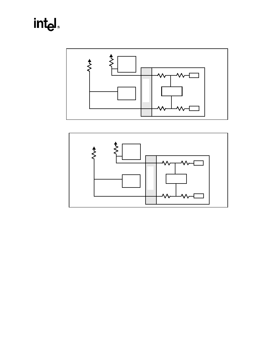
Figure 5.
BSEL[1:0] Example for a 100/133MHz Capable System (100 MHz Processor Installed)
Figure 6.
BSEL[1:0] Example for a 100/133MHz Capable System (133 MHz Processor Installed)
2.9
Test Access Port (TAP) Connection
Due to the voltage levels supported by other components in the Test Access Port (TAP) logic, it is
recommended that the Pentium III processor be first in the TAP chain and followed by any other
components within the system. A translation buffer should be used to connect to the rest of the
chain unless one of the other components is capable of accepting a 2.5 V input. Similar
considerations must be made for TCK, TMS, and TRST#. Two copies of each signal may be
required with each driving a different voltage level.
The Debug Port should be placed at the start and end of the TAP chain with the TDI of the first
component coming from the Debug Port and the TDO from the last component going to the Debug
Port. In a 2-way MP system, be cautious when including an empty SC242 connector in the scan
chain. All connectors in the scan chain must have a processor installed to complete the chain or the
system must support a method to bypass the empty connectors; SC242 terminator substrates should
not connect TDI to TDO in order to avoid placing the TDO pull-up resistors in parallel. See SC242
Terminator Card Design Guidelines (Order Number 243409) for more details.
3.3 Volts
CK133
S
L
O
T
1
Processor
Core
GND
Pentium III Processor
1 K
220
S
C
2
4
2
System
BSEL0
133/100#
GND
0
0
3.3 Volts
BSEL1
220
Shutdown
Logic
3.3 K
3.3 Volts
CK133
S
L
O
T
1
Processor
Core
GND
Pentium III Processor
1 K
220
S
C
2
4
2
System
BSEL0
133/100#
GND
3.3 K
1 K
3.3 Volts
BSEL1
220
Shutdown
Logic
3.3 K
相关PDF资料 |
PDF描述 |
|---|---|
| BX80525U550512E | 32-BIT, 550 MHz, MICROPROCESSOR, XMA |
| BX80525U450512E | 32-BIT, 450 MHz, MICROPROCESSOR, XMA |
| BX80526F500256E | 32-BIT, 500 MHz, MICROPROCESSOR, PPGA370 |
| BX80526F650256E | 32-BIT, 650 MHz, MICROPROCESSOR, PPGA370 |
| BX80526F750256E | 32-BIT, 750 MHz, MICROPROCESSOR, PPGA370 |
相关代理商/技术参数 |
参数描述 |
|---|---|
| BX80525U550256E | 制造商:未知厂家 制造商全称:未知厂家 功能描述:Microprocessor |
| BX80525U600256E | 制造商:未知厂家 制造商全称:未知厂家 功能描述:Microprocessor |
| BX80525U600256EB | 制造商:未知厂家 制造商全称:未知厂家 功能描述:Microprocessor |
| BX80525U650256 | 制造商:未知厂家 制造商全称:未知厂家 功能描述:Microprocessor |
| BX80525U667256 | 制造商:未知厂家 制造商全称:未知厂家 功能描述:Microprocessor |
发布紧急采购,3分钟左右您将得到回复。