- 您现在的位置:买卖IC网 > PDF目录298892 > BX80525U533512E (INTEL CORP) 32-BIT, 533 MHz, MICROPROCESSOR, XMA PDF资料下载
参数资料
| 型号: | BX80525U533512E |
| 厂商: | INTEL CORP |
| 元件分类: | 微控制器/微处理器 |
| 英文描述: | 32-BIT, 533 MHz, MICROPROCESSOR, XMA |
| 文件页数: | 18/94页 |
| 文件大小: | 898K |
| 代理商: | BX80525U533512E |
第1页第2页第3页第4页第5页第6页第7页第8页第9页第10页第11页第12页第13页第14页第15页第16页第17页当前第18页第19页第20页第21页第22页第23页第24页第25页第26页第27页第28页第29页第30页第31页第32页第33页第34页第35页第36页第37页第38页第39页第40页第41页第42页第43页第44页第45页第46页第47页第48页第49页第50页第51页第52页第53页第54页第55页第56页第57页第58页第59页第60页第61页第62页第63页第64页第65页第66页第67页第68页第69页第70页第71页第72页第73页第74页第75页第76页第77页第78页第79页第80页第81页第82页第83页第84页第85页第86页第87页第88页第89页第90页第91页第92页第93页第94页
Pentium
III Processor at 450 MHz, 500 MHz, 533B MHz, 550 MHz, 600/600B MHz
Datasheet
25
NOTES:
1. Unless otherwise noted, all specifications in this table apply to Pentium
III processor frequencies.
2. VIH and VOH for the Pentium III processor may experience excursions of up to 200 mV above VTT for a single system bus
clock. However, input signal drivers must comply with the signal quality specifications in Section 3.0.
3. Minimum and maximum VTT are given in Table 10.
4. Parameter correlated to measure into a 25
resistor terminated to 1.5 V.
5. IOH for the Pentium III processor may experience excursions of up to a 12 mA for a single bus clock.
6. (0
≤ VIN ≤ 2.0 V +5%).
7. (0
≤ VOUT ≤ 2.0 V +5%).
8. Refer to the Pentium III I/O Buffer Models for I/V characteristics.
NOTES:
1. Unless otherwise noted, all specifications in this table apply to all Pentium
III processor frequencies.
2. Parameter measured at 14 mA (for use with TTL inputs).
3. (0
≤ VIN ≤ 2.5 V +5%).
4. (0
≤ VOUT ≤ 2.5 V +5%).
2.12
AGTL+ System Bus Specifications
It is recommended that the AGTL+ bus be routed in a daisy-chain fashion with termination
resistors to V
TT at each end of the signal trace. These termination resistors are placed electrically
between the ends of the signal traces and the V
TT voltage supply and generally are chosen to
approximate the substrate impedance. The valid high and low levels are determined by the input
buffers using a reference voltage called V
REF.
Table 10 lists the nominal specification for the AGTL+ termination voltage (V
TT). The AGTL+
reference voltage (V
REF) is generated on the processor substrate for the processor core, but should
be set to 2/3 V
TT for other AGTL+ logic using a voltage divider on the baseboard. It is important
that the baseboard impedance be specified and held to a ±15% tolerance, and that the intrinsic trace
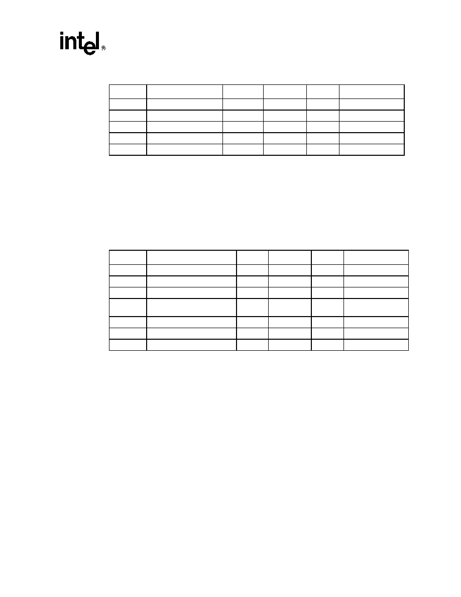
Table 8.
AGTL+ Signal Groups DC Specifications 1, 4, 5
Symbol
Parameter
Min
Max
Unit
Notes
VIL
Input Low Voltage
–0.3
0.82
V
VIH
Input High Voltage
1.22
VTT
V2, 3
Ron
Buffer On Resistance
16.67
8
IL
Leakage Current
±100
A
6
ILO
Output Leakage Current
±15
A
7
Table 9.
Non-AGTL+ Signal Group DC Specifications 1
Symbol
Parameter
Min
Max
Unit
Notes
VIL
Input Low Voltage
–0.3
0.5
V
VIH
Input High Voltage
1.7
2.625
V
2.5 V +5% maximum
VOL
Output Low Voltage
0.4
V
2
VOH
Output High Voltage
N/A
2.625
V
All outputs are
open-drain
IOL
Output Low Current
14
mA
ILI
Input Leakage Current
±100
A
3
ILO
Output Leakage Current
±15
A
4
相关PDF资料 |
PDF描述 |
|---|---|
| BX80525U550512E | 32-BIT, 550 MHz, MICROPROCESSOR, XMA |
| BX80525U450512E | 32-BIT, 450 MHz, MICROPROCESSOR, XMA |
| BX80526F500256E | 32-BIT, 500 MHz, MICROPROCESSOR, PPGA370 |
| BX80526F650256E | 32-BIT, 650 MHz, MICROPROCESSOR, PPGA370 |
| BX80526F750256E | 32-BIT, 750 MHz, MICROPROCESSOR, PPGA370 |
相关代理商/技术参数 |
参数描述 |
|---|---|
| BX80525U550256E | 制造商:未知厂家 制造商全称:未知厂家 功能描述:Microprocessor |
| BX80525U600256E | 制造商:未知厂家 制造商全称:未知厂家 功能描述:Microprocessor |
| BX80525U600256EB | 制造商:未知厂家 制造商全称:未知厂家 功能描述:Microprocessor |
| BX80525U650256 | 制造商:未知厂家 制造商全称:未知厂家 功能描述:Microprocessor |
| BX80525U667256 | 制造商:未知厂家 制造商全称:未知厂家 功能描述:Microprocessor |
发布紧急采购,3分钟左右您将得到回复。