- 您现在的位置:买卖IC网 > PDF目录366628 > C9811X2AYB Up to 5A ULDO linear regulator PDF资料下载
参数资料
| 型号: | C9811X2AYB |
| 英文描述: | Up to 5A ULDO linear regulator |
| 中文描述: | CPU系统时钟发生器| SSOP封装| 56PIN |塑料 |
| 文件页数: | 10/17页 |
| 文件大小: | 232K |
| 代理商: | C9811X2AYB |
Low EMI Clock Generator for Intel
810 Chipset Systems
Cypress Semiconductor Corporation
525 Los Coches St.
Milpitas, CA 95035. Tel: 408-263-6300, Fax: 408-263-6571
http://www.cypress.com
Document#: 38-07052 Rev. **
05/03/2001
Page 10 of 17
APPROVED PRODUCT
C9811x2
Maximum Ratings
Maximum Input Voltage Relative to VSS: VSS - 0.3V
Maximum Input Voltage Relative to VDD: VDD + 0.3V
Storage Temperature:
Operating Temperature:
Maximum ESD protection
Maximum Power Supply:
-65
o
C to + 150
o
C
0
o
C to +85
o
C
2KV
5.5V
This device contains circuitry to protect the inputs
against damage due to high static voltages or electric
field; however, precautions should be taken to avoid
application of any voltage higher than the maximum
rated voltages to this circuit. For proper operation, Vin
and Vout should be constrained to the range:
VSS<(Vin or Vout)<VDD
Unused inputs must always be tied to an appropriate
logic voltage level (either VSS or VDD
).
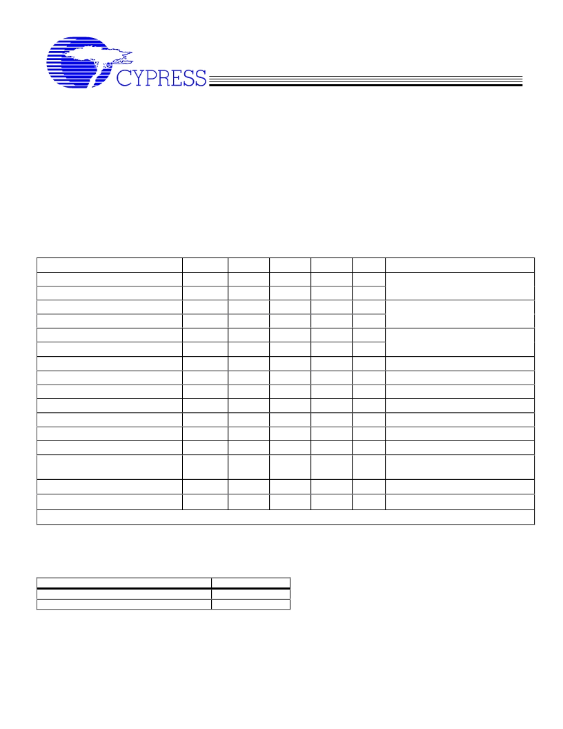
DC Parameters
Characteristic
Input Low Voltage
Input High Voltage
Input Low Voltage
Input High Voltage
Input Low Current (@VIL =VSS)
Input High Current (@VIL =VDD)
Tri-State leakage Current
Dynamic Supply Current
Dynamic Supply Current
Static Supply Current
Input pin capacitance
Output pin capacitance
Pin capacitance
Crystal pin capacitance
Symbol
VIL1
VIH1
VIL2
VIH2
IIL
IIH
Ioz
Idd3.3V
Idd2.5V
Isdd
Cin
Cout
Lpin
Cxtal
Min
Typ
Max
Units
Vdc
Vdc
Vdc
Vdc
μA
μA
μA
mA
mA
mA
pF
pF
nH
pF
Conditions
-
-
-
-
-
1.0
-
1.0
-
-5
5
10
280
100
3.2
5
6
7
38
2.0
-
2.2
-66
note 1
note 2
For internal Pull up resistors, note
1 and note 3
-
-
-
-
-
-
-
-
-
-
-
-
-
-
Sel1 = Sel0 = 1, note 4
Sel1 = Sel0 = 1, note 4
PD# = 0, Sel1 = Sel0 = x, note 4
32
34
Measured from Pin to Ground.
note 5
Crystal DC Bias Voltage
Crystal Startup time
V
BIAS
Txs
0.3Vdd
-
Vdd/2
-
0.7Vdd
40
V
μ
S
From Stable 3.3V power supply.
VDD=VDDS = 3.3V
±
5
%, VDDC = VDDI = 2.5
±
5%, TA = 0o to +70oC
Applicable to input signals: Sel(0:1), PD#
Applicable to Sdata, and Sclk.
Although internal pull-up resistors have a typical value of 250K, this value may vary between 200K and 500K.
All outputs loaded as per table 3.
Although the device will reliably interface with crystals of a 17pF
–
20pF C
L
range, it is optimized to interface with a typical C
L
= 18pF
crystal specifications.
Clock name
Max Load (in pF)
CPU, IOAPIC, REF, USB (0:1)
20
PCI, SDRAM, 3V66(0,1)
30
Table 5.
Note1:
Note2:
Note3:
Note4:
Note5:
相关PDF资料 |
PDF描述 |
|---|---|
| C9812DYB | Up to 5A ULDO linear regulator |
| C9815DY | Up to 5A ULDO linear regulator |
| C9821GQ | Up to 5A ULDO linear regulator |
| C9822EQ | Up to 5A ULDO linear regulator |
| C9827JT | Up to 5A ULDO linear regulator |
相关代理商/技术参数 |
参数描述 |
|---|---|
| C9812 | 制造商:CYPRESS 制造商全称:Cypress Semiconductor 功能描述:Low EMI Clock Generator for Intel 810E Chipset Systems |
| C9812DYB | 制造商:未知厂家 制造商全称:未知厂家 功能描述:CPU SYSTEM CLOCK GENERATOR|SSOP|56PIN|PLASTIC |
| C98130-A1231-C30 | 制造商:Siemens 功能描述: |
| C9815DY | 制造商:未知厂家 制造商全称:未知厂家 功能描述:CPU SYSTEM CLOCK GENERATOR|SSOP|56PIN|PLASTIC |
| C981FFN-CTN | 制造商:Thomas & Betts 功能描述:1" FSC 1-GANG WP BOX 18 CU IN-CAN |
发布紧急采购,3分钟左右您将得到回复。