- 您现在的位置:买卖IC网 > PDF目录366628 > C9811X2AYB Up to 5A ULDO linear regulator PDF资料下载
参数资料
| 型号: | C9811X2AYB |
| 英文描述: | Up to 5A ULDO linear regulator |
| 中文描述: | CPU系统时钟发生器| SSOP封装| 56PIN |塑料 |
| 文件页数: | 2/17页 |
| 文件大小: | 232K |
| 代理商: | C9811X2AYB |
Low EMI Clock Generator for Intel
810 Chipset Systems
Cypress Semiconductor Corporation
525 Los Coches St.
Milpitas, CA 95035. Tel: 408-263-6300, Fax: 408-263-6571
http://www.cypress.com
Document#: 38-07052 Rev. **
05/03/2001
Page 2 of 17
APPROVED PRODUCT
C9811x2
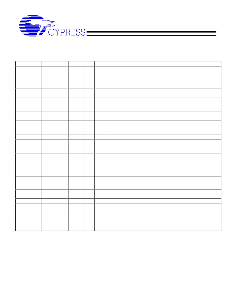
Pin Description
PIN No.
1
Pin Name
ASEL/REF
PWR
VDD
I/O
I/O
TYPE
Description
3.3V 14.318 MHz clock output. This pin also serves as the
select strap for IOAPIC clock frequency. If strapped low during
power up, IOAPIC clocks run at PCI/2 (16.6 MHz). If not
strapped, it runs at 33 MHz. This pin has a 50K internal pull-up
(+/- 20K).
14.318MHz Crystal input
14.318MHz Crystal output
3.3V PCI clock outputs
3
4
11, 12, 13,
15, 16, 18,
19, 20
7, 8
25, 26
28, 29
XIN
XOUT
PCI0/ICH
PCI(1..7)
VDD
VDD
VDD
I
OSC1
O
O
3V66(0,1)
USB (0:1)
SEL(0,1)
VDD
VDD
VDD
O
O
I
3.3V Fixed 66.6 MHz clock outputs
3.3V Fixed 48 MHz clock outputs
3.3V LVTTL compatible inputs for logic selection. Has an
internal pull-up (Typ. 250K
)
I
2
C compatible SDATA input. Has an internal pull-up (>100K
)
I
2
C compatible SCLK input. Has an internal pull-up (>100K
)
3.3V LVTTL compatible input. Device enters powerdown mode
When held LOW. Has an internal pull-up (>100K
)
3.3V output running 100MHz
3.3V output running 100MHz. All SDRAM outputs can be turned
off through SMBUS.
30
31
32
SDATA
SCLK
PD#
VDD
VDD
VDD
I
I
I
34
36, 37, 39,
40, 42, 43,
45, 46
49, 50, 52
DCLK
SDRAM(7..0)
VDD
VDDS
O
O
CPU(2)_ITP,
CPU(1,0)
IOAPIC(1,0)
VDDC
O
2.5V Host bus clock outputs. 66 or 100MHz depending on state
of SEL0 and SEL1 pins.
2.5V clock outputs running rising edge synchronous with the
PCI clock frequency. 16.67 MHz or 33.3 MHz dependent on
power up strapping of REF (Pin 1).
3.3V Power Supply
54, 55
VDDI
O
2, 9, 10, 21,
27
22
23
51, 53
5, 6,14, 17,
24, 35, 41,
47, 48, 56
33, 38, 44
A bypass capacitor (0.1
μ
F) should be placed as close as possible to each positive power pin. If these bypass capacitors
are not close to the pins their high frequency filtering characteristic will be cancelled by the lead inductance of the traces.
VDD
-
VDDA
VSSA
VDDC, VDDI
VSS
-
-
-
-
P
P
P
P
Analog circuitry 3.3V Power Supply
Analog circuitry power supply Ground pins.
2.5V Power Supply
’
s
Common Ground pins.
-
VDDS
-
P
-
3.3V power support for SDRAM clock output drivers.
相关PDF资料 |
PDF描述 |
|---|---|
| C9812DYB | Up to 5A ULDO linear regulator |
| C9815DY | Up to 5A ULDO linear regulator |
| C9821GQ | Up to 5A ULDO linear regulator |
| C9822EQ | Up to 5A ULDO linear regulator |
| C9827JT | Up to 5A ULDO linear regulator |
相关代理商/技术参数 |
参数描述 |
|---|---|
| C9812 | 制造商:CYPRESS 制造商全称:Cypress Semiconductor 功能描述:Low EMI Clock Generator for Intel 810E Chipset Systems |
| C9812DYB | 制造商:未知厂家 制造商全称:未知厂家 功能描述:CPU SYSTEM CLOCK GENERATOR|SSOP|56PIN|PLASTIC |
| C98130-A1231-C30 | 制造商:Siemens 功能描述: |
| C9815DY | 制造商:未知厂家 制造商全称:未知厂家 功能描述:CPU SYSTEM CLOCK GENERATOR|SSOP|56PIN|PLASTIC |
| C981FFN-CTN | 制造商:Thomas & Betts 功能描述:1" FSC 1-GANG WP BOX 18 CU IN-CAN |
发布紧急采购,3分钟左右您将得到回复。