- 您现在的位置:买卖IC网 > PDF目录16832 > CRD5463PM-Z (Cirrus Logic Inc)REFERENCE DESIGN FOR POWER METER PDF资料下载
参数资料
| 型号: | CRD5463PM-Z |
| 厂商: | Cirrus Logic Inc |
| 文件页数: | 21/46页 |
| 文件大小: | 0K |
| 描述: | REFERENCE DESIGN FOR POWER METER |
| 标准包装: | 1 |
| 主要目的: | 电源管理,电度表/功率表 |
| 嵌入式: | 是,MCU,8 位 |
| 已用 IC / 零件: | CS5463 |
| 主要属性: | 单相功率表 |
| 次要属性: | 90 ~ 260 VAC |
| 已供物品: | 模块,适配器,线缆,电源线 |
| 其它名称: | 598-1943 |
第1页第2页第3页第4页第5页第6页第7页第8页第9页第10页第11页第12页第13页第14页第15页第16页第17页第18页第19页第20页当前第21页第22页第23页第24页第25页第26页第27页第28页第29页第30页第31页第32页第33页第34页第35页第36页第37页第38页第39页第40页第41页第42页第43页第44页第45页第46页
�� �
�
�CS5463�
�drive� the� device� from� an� external� clock� source,� XOUT�
�should� be� left� unconnected� while� XIN� is� driven� by� the�
�external� circuitry.� There� is� an� amplifier� between� XIN� and�
�the� digital� section� which� provides� CMOS� level� signals.�
�This� amplifier� works� with� sinusoidal� inputs� so� there� are�
�no� problems� with� slow� edge� times.�
�The� CS5463� can� be� driven� by� an� external� oscillator�
�ranging� from� 2.5� to� 20� MHz,� but� the� K� divider� value� must�
�be� set� such� that� the� internal� MCLK� will� run� somewhere�
�between� 2.5� MHz� and� 5� MHz.� The� K� divider� value� is� set�
�with� the� K[3:0]� bits� in� the� Configuration� Register� .� As� an�
�example,� if� XIN� =� MCLK� =� 15� MHz,� and� K� is� set� to� 5,�
�DCLK� will� equal� 3� MHz,� which� is� a� valid� value� for� DCLK.�
�5.13� Event� Handler�
�The� INT� pin� is� used� to� indicate� that� an� internal� error� or�
�event� has� taken� place� in� the� CS5463.� Writing� a� logic� 1�
�to� any� bit� in� the� Mask� Register� allows� the� corresponding�
�bit� in� the� Status� Register� to� activate� the� INT� pin.� The� in-�
�terrupt� condition� is� cleared� by� writing� a� logic� 1� to� the� bit�
�that� has� been� set� in� the� Status� Register� .�
�The� behavior� of� the� INT� pin� is� controlled� by� the� IMODE�
�and� IINV� bits� of� the� Configuration� Register� .�
�INTERRUPT HANDLER ROUTINE� :�
�4)� Read� the� Status� Register.�
�5)� Disable� all� interrupts.�
�6)� Branch� to� the� proper� interrupt� service� routine.�
�7)� Clear� the� Status� Register� by� writing� back� the� read�
�value� in� step� 4.�
�8)� Re-enable� interrupt�
�9)� Return� from� interrupt� service� routine.�
�This� handshaking� procedure� ensures� that� any� new� in-�
�terrupts� activated� between� steps� 4� and� 7� are� not� lost�
�(cleared)� by� step� 7.�
�5.14� Serial� Port� Overview�
�The� CS5463� incorporates� a� serial� port� transmit� and� re-�
�ceive� buffer� with� a� command� decoder� that� interprets�
�one-byte� (8-bit)� commands� as� they� are� received.� There�
�are� four� types� of� commands:� instructions,� synchroniz-�
�ing,� register� writes,� and� register� reads� (See� Section�
�5.16� Commands� on� page� 23).�
�Instructions� are� one� byte� in� length� and� will� interrupt� any�
�instruction� currently� executing.� Instructions� do� not� affect�
�IMODE�
�0�
�IINV�
�0�
�INT� Pin�
�Active-low� Level�
�register� reads� currently� being� transmitted.�
�Synchronizing� commands� are� one� byte� in� length� and�
�only� affect� the� serial� interface.� Synchronizing� com-�
�mands� do� not� affect� operations� currently� in� progress.�
�0�
�1�
�Active-high� Level�
�Register� writes� must� be� followed� by� three� bytes� of� data.�
�Register� reads� can� return� up� to� four� bytes� of� data.�
�1�
�1�
�0�
�1�
�Low� Pulse�
�High� Pulse�
�Commands� and� data� are� transferred� most-significant� bit�
�(MSB)� first.� Figure� 1� on� page� 12,� defines� the� serial� port�
�timing� and� required� sequence� necessary� for� writing� to�
�and� reading� from� the� serial� port� receive� and� transmit�
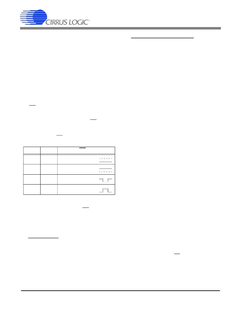
�Table� 4.� Interrupt� Configuration�
�If� the� interrupt� output� signal� format� is� set� for� either� falling�
�or� rising� edge,� the� duration� of� the� INT� pulse� will� be� at�
�least� one� DCLK� cycle� (DCLK� =� MCLK/K).�
�5.13.1� Typical� Interrupt� Handler�
�The� steps� below� show� how� interrupts� can� be� handled.�
�INITIALIZATION� :�
�1)� All� Status� bits� are� cleared� by� writing� 0xFFFFFF� to�
�the� Status� Register.�
�2)� The� condition� bits� which� will� be� used� to� generate�
�interrupts� are� then� set� to� logic� 1� in� the� Mask� Reg-�
�ister.�
�3)� Enable� interrupts.�
�DS678F3�
�buffer,� respectively.� While� reading� data� from� the� serial�
�port,� commands� and� data� can� be� written� simultaneous-�
�ly.� Starting� a� new� register� read� command� while� data� is�
�being� read� will� terminate� the� current� read� in� progress.�
�This� is� acceptable� if� the� remainder� of� the� current� read�
�data� is� not� needed.� During� data� reads,� the� serial� port� re-�
�quires� input� data.� If� a� new� command� and� data� is� not�
�sent,� SYNC0� or� SYNC1� must� be� sent.�
�5.14.1� Serial� Port� Interface�
�The� serial� port� interface� is� a� “4-wire”� synchronous� serial�
�communications� interface.� The� interface� is� enabled� to�
�start� excepting� SCLKs� when� CS� (Chip� Select)� is� assert-�
�ed� (logic� 0).� SCLK� (Serial� bit-clock)� is� a� Schmitt-trigger�
�input� that� is� used� to� strobe� the� data� on� SDI� (Serial� Data�
�In)� into� the� receive� buffer� and� out� of� the� transmit� buffer�
�onto� SDO� (Serial� Data� Out).�
�21�
�相关PDF资料 |
PDF描述 |
|---|---|
| M1AXA-1436R | IDC CABLE - MSC14A/MC14M/X |
| 0982660228 | CBL 22POS .5MM JMPR TYPE D 1.18" |
| 301A034-4-0 | BOOT MOLDED |
| H3DDS-1418M | IDC CABLE - HKR14S/AE14M/HKR14S |
| 0982660227 | CBL 22POS .5MM JMPR TYPE A 1.18" |
相关代理商/技术参数 |
参数描述 |
|---|---|
| CRD5490-Z | 功能描述:电源管理IC开发工具 CS5463 Pwr Meas/Mntr Reference Design RoHS:否 制造商:Maxim Integrated 产品:Evaluation Kits 类型:Battery Management 工具用于评估:MAX17710GB 输入电压: 输出电压:1.8 V |
| CRD5AS-12B | 制造商:RENESAS 制造商全称:Renesas Technology Corp 功能描述:Reverse Conducting Thyristor Medium Power Use |
| CRD5AS-12B#B00 | 功能描述:SCR 600V 7.8A Sensitive Gate Surface Mount MP-3A 制造商:renesas electronics america 系列:- 包装:管件 零件状态:有效 电压 - 断态:600V 电压 - 栅极触发(Vgt)(最大值):800mV 电流 - 栅极触发(Igt)(最大值):100μA 电压 - 通态(Vtm)(最大值):1.8V 电流 - 通态(It(AV))(最大值):5A 电流 - 通态(It(RMS))(最大值):7.8A 电流 - 保持(Ih)(最大值):3mA 电流 - 断态(最大值):2mA 电流 - 不重复浪涌 50,60Hz(Itsm):90A @ 60Hz SCR 类型:灵敏栅极 工作温度:-40°C ~ 150°C 安装类型:表面贴装 封装/外壳:TO-252-3,DPak(2 引线+接片),SC-63 供应商器件封装:MP-3A 标准包装:1 |
| CRD5AS-12BB00 | 制造商:RENESAS 制造商全称:Renesas Technology Corp 功能描述:Reverse Conducting Thyristor Medium Power Use |
| CRD5AS-12B-T13B00 | 制造商:RENESAS 制造商全称:Renesas Technology Corp 功能描述:Reverse Conducting Thyristor Medium Power Use |
发布紧急采购,3分钟左右您将得到回复。