- 您现在的位置:买卖IC网 > PDF目录295373 > CY7C1157V18-333BZXI (CYPRESS SEMICONDUCTOR CORP) 18-Mbit DDR-II+ SRAM 2-Word Burst Architecture (2.0 Cycle Read Latency) PDF资料下载
参数资料
| 型号: | CY7C1157V18-333BZXI |
| 厂商: | CYPRESS SEMICONDUCTOR CORP |
| 元件分类: | SRAM |
| 英文描述: | 18-Mbit DDR-II+ SRAM 2-Word Burst Architecture (2.0 Cycle Read Latency) |
| 中文描述: | 2M X 9 DDR SRAM, 0.45 ns, PBGA165 |
| 封装: | 13 X 15 MM, 1.40 MM HEIGHT, LEAD FREE, MO-216, FBGA-165 |
| 文件页数: | 9/27页 |
| 文件大小: | 645K |
| 代理商: | CY7C1157V18-333BZXI |
第1页第2页第3页第4页第5页第6页第7页第8页当前第9页第10页第11页第12页第13页第14页第15页第16页第17页第18页第19页第20页第21页第22页第23页第24页第25页第26页第27页
CY7C1146V18, CY7C1157V18
CY7C1148V18, CY7C1150V18
Document Number: 001-06621 Rev. *D
Page 17 of 27
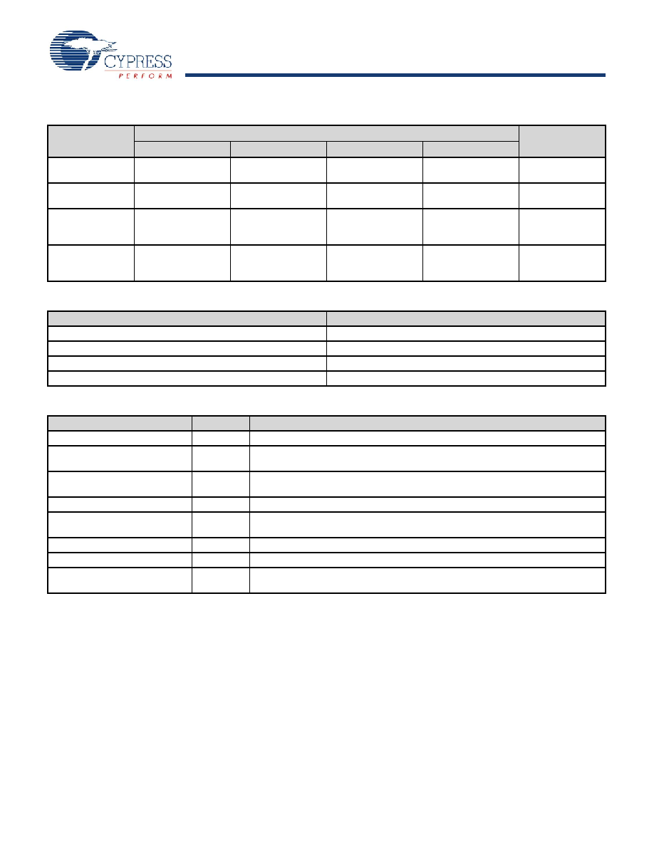
Identification Register Definitions
Instruction Field
Value
Description
CY7C1146V18
CY7C1157V18
CY7C1148V18
CY7C1150V18
Revision Number
(31:29)
000
Version number.
Cypress Device ID
(28:12)
11010111100000101
11010111100001101
11010111100010101
11010111100100101 Defines the type of
SRAM.
Cypress JEDEC ID
(11:1)
00000110100
Allows unique
identification of
SRAM vendor.
ID Register
Presence (0)
1
Indicates the
presence of an ID
register.
Scan Register Sizes
Register Name
Bit Size
Instruction
3
Bypass
1
ID
32
Boundary Scan
107
Instruction Codes
Instruction
Code
Description
EXTEST
000
Captures the Input Output ring contents.
IDCODE
001
Loads the ID register with the vendor ID code and places the register between TDI
and TDO. This operation does not affect SRAM operation.
SAMPLE Z
010
Captures the Input Output contents. Places the boundary scan register between TDI
and TDO. Forces all SRAM output drivers to a High-Z state.
RESERVED
011
Do Not Use: This instruction is reserved for future use.
SAMPLE/PRELOAD
100
Captures the Input Output ring contents. Places the boundary scan register between
TDI and TDO. Does not affect the SRAM operation.
RESERVED
101
Do Not Use: This instruction is reserved for future use.
RESERVED
110
Do Not Use: This instruction is reserved for future use.
BYPASS
111
Places the bypass register between TDI and TDO. This operation does not affect
SRAM operation.
相关PDF资料 |
PDF描述 |
|---|---|
| CY7C1157V18-375BZC | 18-Mbit DDR-II+ SRAM 2-Word Burst Architecture (2.0 Cycle Read Latency) |
| CY7C1157V18-375BZI | 18-Mbit DDR-II+ SRAM 2-Word Burst Architecture (2.0 Cycle Read Latency) |
| CY7C1157V18-375BZXC | 18-Mbit DDR-II+ SRAM 2-Word Burst Architecture (2.0 Cycle Read Latency) |
| CY7C1157V18-375BZXI | 18-Mbit DDR-II+ SRAM 2-Word Burst Architecture (2.0 Cycle Read Latency) |
| CY7C1157V18 | 18-Mbit DDR-II+ SRAM 2-Word Burst Architecture (2.0 Cycle Read Latency) |
相关代理商/技术参数 |
参数描述 |
|---|---|
| CY7C1163KV18-400BZI | 功能描述:静态随机存取存储器 18MB (1Mx18) 1.8v 400MHz DDR II 静态随机存取存储器 RoHS:否 制造商:Cypress Semiconductor 存储容量:16 Mbit 组织:1 M x 16 访问时间:55 ns 电源电压-最大:3.6 V 电源电压-最小:2.2 V 最大工作电流:22 uA 最大工作温度:+ 85 C 最小工作温度:- 40 C 安装风格:SMD/SMT 封装 / 箱体:TSOP-48 封装:Tray |
| CY7C1163KV18-450BZC | 功能描述:静态随机存取存储器 18MB (1Mx18) 1.8v 450MHz DDR II 静态随机存取存储器 RoHS:否 制造商:Cypress Semiconductor 存储容量:16 Mbit 组织:1 M x 16 访问时间:55 ns 电源电压-最大:3.6 V 电源电压-最小:2.2 V 最大工作电流:22 uA 最大工作温度:+ 85 C 最小工作温度:- 40 C 安装风格:SMD/SMT 封装 / 箱体:TSOP-48 封装:Tray |
| CY7C1163KV18-550BZC | 功能描述:静态随机存取存储器 18MB (1Mx18) 1.8v 550MHz DDR II 静态随机存取存储器 RoHS:否 制造商:Cypress Semiconductor 存储容量:16 Mbit 组织:1 M x 16 访问时间:55 ns 电源电压-最大:3.6 V 电源电压-最小:2.2 V 最大工作电流:22 uA 最大工作温度:+ 85 C 最小工作温度:- 40 C 安装风格:SMD/SMT 封装 / 箱体:TSOP-48 封装:Tray |
| CY7C11651KV18-400BZC | 功能描述:静态随机存取存储器 Sync 静态随机存取存储器 QDR RoHS:否 制造商:Cypress Semiconductor 存储容量:16 Mbit 组织:1 M x 16 访问时间:55 ns 电源电压-最大:3.6 V 电源电压-最小:2.2 V 最大工作电流:22 uA 最大工作温度:+ 85 C 最小工作温度:- 40 C 安装风格:SMD/SMT 封装 / 箱体:TSOP-48 封装:Tray |
| CY7C11651KV18-400BZXC | 功能描述:IC SRAM 18MBIT 400MHZ 165-FPBGA RoHS:是 类别:集成电路 (IC) >> 存储器 系列:- 标准包装:150 系列:- 格式 - 存储器:EEPROMs - 串行 存储器类型:EEPROM 存储容量:4K (2 x 256 x 8) 速度:400kHz 接口:I²C,2 线串口 电源电压:2.5 V ~ 5.5 V 工作温度:-40°C ~ 85°C 封装/外壳:8-VFDFN 裸露焊盘 供应商设备封装:8-DFN(2x3) 包装:管件 产品目录页面:1445 (CN2011-ZH PDF) |
发布紧急采购,3分钟左右您将得到回复。