- 您现在的位置:买卖IC网 > PDF目录298976 > CY7C2561KV18-450BZC (CYPRESS SEMICONDUCTOR CORP) 8M X 8 QDR SRAM, 0.37 ns, PBGA165 PDF资料下载
参数资料
| 型号: | CY7C2561KV18-450BZC |
| 厂商: | CYPRESS SEMICONDUCTOR CORP |
| 元件分类: | SRAM |
| 英文描述: | 8M X 8 QDR SRAM, 0.37 ns, PBGA165 |
| 封装: | 15 X 13 MM, 1.4 MM HEIGHT, FBGA-165 |
| 文件页数: | 27/29页 |
| 文件大小: | 839K |
| 代理商: | CY7C2561KV18-450BZC |
第1页第2页第3页第4页第5页第6页第7页第8页第9页第10页第11页第12页第13页第14页第15页第16页第17页第18页第19页第20页第21页第22页第23页第24页第25页第26页当前第27页第28页第29页
PRELIMINARY
CY7C2561KV18, CY7C2576KV18
CY7C2563KV18, CY7C2565KV18
Document Number: 001-15887 Rev. *E
Page 7 of 29
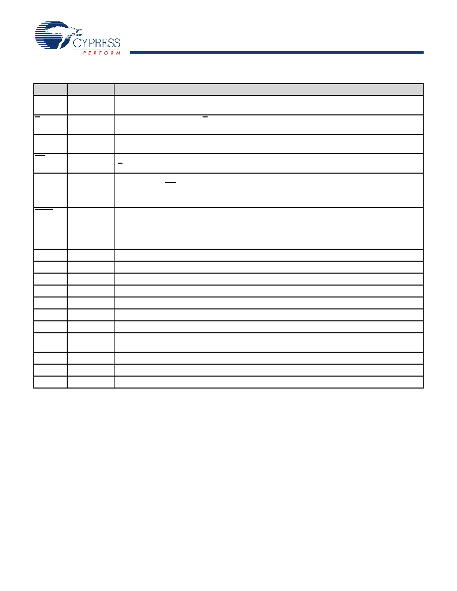
K
Input Clock
Positive Input Clock Input. The rising edge of K is used to capture synchronous inputs to the device
and to drive out data through Q[x:0]. All accesses are initiated on the rising edge of K.
K
Input Clock
Negative Input Clock Input. K is used to capture synchronous inputs being presented to the device and
to drive out data through Q[x:0].
CQ
Echo Clock
Synchronous Echo Clock Outputs. This is a free running clock and is synchronized to the input clock
(K) of the QDR-II+. The timings for the echo clocks are shown in the Switching Characteristics on page 24.
CQ
Echo Clock
Synchronous Echo Clock Outputs. This is a free running clock and is synchronized to the input clock
(K) of the QDR-II+.The timings for the echo clocks are shown in the Switching Characteristics on page 24.
ZQ
Input
Output Impedance Matching Input. This input is used to tune the device outputs to the system data bus
impedance. CQ, CQ, and Q[x:0] output impedance are set to 0.2 x RQ, where RQ is a resistor connected
between ZQ and ground. Alternatively, this pin can be connected directly to VDDQ, which enables the
minimum impedance mode. This pin cannot be connected directly to GND or left unconnected.
DOFF
Input
PLL Turn Off
Active LOW. Connecting this pin to ground turns off the PLL inside the device. The timings
in the PLL turned off operation differs from those listed in this data sheet. For normal operation, this pin
can be connected to a pull up through a 10 K
Ω or less pull up resistor. The device behaves in QDR-I
mode when the PLL is turned off. In this mode, the device can be operated at a frequency of up to 167
MHz with QDR-I timing.
TDO
Output
TDO for JTAG.
TCK
Input
TCK Pin for JTAG.
TDI
Input
TDI Pin for JTAG.
TMS
Input
TMS Pin for JTAG.
NC
N/A
Not Connected to the Die. Can be tied to any voltage level.
NC/144M
N/A
Not Connected to the Die. Can be tied to any voltage level.
NC/288M
N/A
Not Connected to the Die. Can be tied to any voltage level.
VREF
Input-
Reference
Reference Voltage Input. Static input used to set the reference level for HSTL inputs, outputs, and AC
measurement points.
VDD
Power Supply Power Supply Inputs to the Core of the Device.
VSS
Ground
Ground for the Device.
VDDQ
Power Supply Power Supply Inputs for the Outputs of the Device.
Table 2. Pin Definitions (continued)
Pin Name
IO
Pin Description
相关PDF资料 |
PDF描述 |
|---|---|
| CY7C2566KV18-450BZI | 8M X 8 DDR SRAM, 0.37 ns, PBGA165 |
| CY7C293AL-35WC | 2K X 8 UVPROM, 35 ns, CDIP24 |
| CY7C474-15DI | 32K X 9 OTHER FIFO, 15 ns, CDIP28 |
| CY7C474-15PI | 32K X 9 OTHER FIFO, 15 ns, PDIP28 |
| CZ12010T0050GBK | 0 MHz - 3000 MHz 50 ohm RF/MICROWAVE TERMINATION |
相关代理商/技术参数 |
参数描述 |
|---|---|
| CY7C2562XV18-366BZXC | 功能描述:静态随机存取存储器 72MB (4Mx18) 1.8v 366MHz QDR II 静态随机存取存储器 RoHS:否 制造商:Cypress Semiconductor 存储容量:16 Mbit 组织:1 M x 16 访问时间:55 ns 电源电压-最大:3.6 V 电源电压-最小:2.2 V 最大工作电流:22 uA 最大工作温度:+ 85 C 最小工作温度:- 40 C 安装风格:SMD/SMT 封装 / 箱体:TSOP-48 封装:Tray |
| CY7C2562XV18-450BZXC | 功能描述:静态随机存取存储器 72MB (4Mx18) 1.8v 450MHz QDR II 静态随机存取存储器 RoHS:否 制造商:Cypress Semiconductor 存储容量:16 Mbit 组织:1 M x 16 访问时间:55 ns 电源电压-最大:3.6 V 电源电压-最小:2.2 V 最大工作电流:22 uA 最大工作温度:+ 85 C 最小工作温度:- 40 C 安装风格:SMD/SMT 封装 / 箱体:TSOP-48 封装:Tray |
| CY7C25632KV18-400BZC | 功能描述:静态随机存取存储器 72MB (4Mx18) 1.8v 400MHz QDR II 静态随机存取存储器 RoHS:否 制造商:Cypress Semiconductor 存储容量:16 Mbit 组织:1 M x 16 访问时间:55 ns 电源电压-最大:3.6 V 电源电压-最小:2.2 V 最大工作电流:22 uA 最大工作温度:+ 85 C 最小工作温度:- 40 C 安装风格:SMD/SMT 封装 / 箱体:TSOP-48 封装:Tray |
| CY7C25632KV18-400BZXI | 功能描述:静态随机存取存储器 72MB (4Mx18) 1.8v 400MHz QDR II 静态随机存取存储器 RoHS:否 制造商:Cypress Semiconductor 存储容量:16 Mbit 组织:1 M x 16 访问时间:55 ns 电源电压-最大:3.6 V 电源电压-最小:2.2 V 最大工作电流:22 uA 最大工作温度:+ 85 C 最小工作温度:- 40 C 安装风格:SMD/SMT 封装 / 箱体:TSOP-48 封装:Tray |
| CY7C25632KV18-450BZC | 功能描述:静态随机存取存储器 72MB (4Mx18) 1.8v 450MHz QDR II 静态随机存取存储器 RoHS:否 制造商:Cypress Semiconductor 存储容量:16 Mbit 组织:1 M x 16 访问时间:55 ns 电源电压-最大:3.6 V 电源电压-最小:2.2 V 最大工作电流:22 uA 最大工作温度:+ 85 C 最小工作温度:- 40 C 安装风格:SMD/SMT 封装 / 箱体:TSOP-48 封装:Tray |
发布紧急采购,3分钟左右您将得到回复。