- 您现在的位置:买卖IC网 > PDF目录17065 > DC939A (Linear Technology)BOARD DELTA SIGMA ADC LTC2484 PDF资料下载
参数资料
| 型号: | DC939A |
| 厂商: | Linear Technology |
| 文件页数: | 17/42页 |
| 文件大小: | 0K |
| 描述: | BOARD DELTA SIGMA ADC LTC2484 |
| 软件下载: | QuikEval System |
| 设计资源: | DC939A Design File DC939A Schematic |
| 标准包装: | 1 |
| 系列: | Easy Drive™, QuikEval™ |
| ADC 的数量: | 1 |
| 位数: | 24 |
| 采样率(每秒): | 6.8 |
| 数据接口: | MICROWIRE?,串行,SPI? |
| 工作温度: | 0°C ~ 70°C |
| 已用 IC / 零件: | LTC2484 |
| 已供物品: | 板 |
| 相关产品: | LTC2484CDD#TRPBF-ND - IC ADC 24BIT 10-DFN LTC2484IDD#TRPBF-ND - IC ADC 24BIT 10-DFN LTC2484IDD#PBF-ND - IC ADC 24BIT 10-DFN LTC2484CDD#PBF-ND - IC ADC 24BIT 10-DFN |
第1页第2页第3页第4页第5页第6页第7页第8页第9页第10页第11页第12页第13页第14页第15页第16页当前第17页第18页第19页第20页第21页第22页第23页第24页第25页第26页第27页第28页第29页第30页第31页第32页第33页第34页第35页第36页第37页第38页第39页第40页第41页第42页
LTC2484
24
2484fd
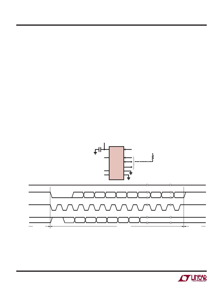
APPLICATIONS INFORMATION
Internal Serial Clock, 3-Wire I/O,
Continuous Conversion
This timing mode uses a 3-wire interface. The conversion
result is shifted out of the device by an internally gener-
ated serial clock (SCK) signal, see Figure 10. CS may be
permanently tied to ground, simplifying the user interface
or transmission over an isolation barrier.
The internal serial clock mode is selected at the end of the
power-on reset (POR) cycle. The POR cycle is concluded
approximately 1ms after VCC exceeds 2V. An internal weak
pull-up is active during the POR cycle; therefore, the internal
serial clock timing mode is automatically selected if SCK
is not externally driven LOW (if SCK is loaded such that
the internal pull-up cannot pull the pin HIGH, the external
SCK mode will be selected).
During the conversion, the SCK and the serial data output
pin (SDO) are HIGH (EOC = 1). Once the conversion is
complete, SCK and SDO go LOW (EOC = 0) indicating
the conversion has nished and the device has entered
the low power sleep state. The part remains in the sleep
state a minimum amount of time (1/2 the internal SCK
period) then immediately begins outputting data. The
data input/output cycle begins on the rst rising edge of
SCK and ends after the 32nd rising edge. The input data
is then shifted in via the SDI pin on the rising edge of
SCK (including the rst rising edge) and the output data
is shifted out of the SDO pin on each falling edge of SCK.
The internally generated serial clock is output to the SCK
pin. This signal may be used to shift the conversion result
into external circuitry. EOC can be latched on the rst ris-
ing edge of SCK and the last bit of the conversion result
can be latched on the 32nd rising edge of SCK. After the
32nd rising edge, SDO goes HIGH (EOC = 1) indicating a
new conversion is in progress. SCK remains HIGH during
the conversion.
EN
GS2
GS1
GS0
IM
FA
FB
SPD
SDI*
DON’T CARE
SDO
SCK
(INTERNAL)
CS
LSB
MSB
SIG
BIT 4
BIT 0
IM
BIT 19
BIT 18
BIT 17
BIT 16
BIT 20
BIT 21
BIT 22
EOC
BIT 23
DATA OUTPUT
CONVERSION
2484 F10
VCC
fO
VREF
IN+
IN–
SCK
SDI
SDO
CS
GND
210
INT/EXT CLOCK
3
4
5
9
7
8
6
1
REFERENCE
VOLTAGE
0.1V TO VCC
ANALOG
INPUT
1μF
2.7V TO 5.5V
LTC2484
3-WIRE
SPI INTERFACE
10k
VCC
Figure 10. Internal Serial Clock, CS = 0 Continuous Operation
相关PDF资料 |
PDF描述 |
|---|---|
| LGU2W680MELY | CAP ALUM 68UF 450V 20% SNAP |
| EVAL-AD5516-1EBZ | BOARD EVAL FOR AD5516-1 2.5V |
| EBA22DRMN | CONN EDGECARD 44POS .125 SQ WW |
| SDR0302-330KL | INDUCTOR POWER 33UH 0.42A 0302 |
| EVAL-AD5516-2EBZ | BOARD EVALUATION FOR AD5516-2 |
相关代理商/技术参数 |
参数描述 |
|---|---|
| DC940KB-GB | 制造商:DEWALT 功能描述:DRILL 12V |
| DC941A | 功能描述:BOARD DELTA SIGMA ADC LTC2482 RoHS:是 类别:编程器,开发系统 >> 评估板 - 模数转换器 (ADC) 系列:Easy Drive™, QuikEval™ 产品培训模块:Obsolescence Mitigation Program 标准包装:1 系列:- ADC 的数量:1 位数:12 采样率(每秒):94.4k 数据接口:USB 输入范围:±VREF/2 在以下条件下的电源(标准):- 工作温度:-40°C ~ 85°C 已用 IC / 零件:MAX11645 已供物品:板,软件 |
| DC945KB | 制造商:DEWALT 功能描述:DRILL KIT CORDLESS 12V |
| DC945KB-GB | 制造商:DEWALT 功能描述:DRILL 12V |
| DC-9-500-2.1P | 制造商:SR COMPONENTS 功能描述: 制造商:SR Components Inc 功能描述: |
发布紧急采购,3分钟左右您将得到回复。