- 您现在的位置:买卖IC网 > PDF目录17065 > DC939A (Linear Technology)BOARD DELTA SIGMA ADC LTC2484 PDF资料下载
参数资料
| 型号: | DC939A |
| 厂商: | Linear Technology |
| 文件页数: | 5/42页 |
| 文件大小: | 0K |
| 描述: | BOARD DELTA SIGMA ADC LTC2484 |
| 软件下载: | QuikEval System |
| 设计资源: | DC939A Design File DC939A Schematic |
| 标准包装: | 1 |
| 系列: | Easy Drive™, QuikEval™ |
| ADC 的数量: | 1 |
| 位数: | 24 |
| 采样率(每秒): | 6.8 |
| 数据接口: | MICROWIRE?,串行,SPI? |
| 工作温度: | 0°C ~ 70°C |
| 已用 IC / 零件: | LTC2484 |
| 已供物品: | 板 |
| 相关产品: | LTC2484CDD#TRPBF-ND - IC ADC 24BIT 10-DFN LTC2484IDD#TRPBF-ND - IC ADC 24BIT 10-DFN LTC2484IDD#PBF-ND - IC ADC 24BIT 10-DFN LTC2484CDD#PBF-ND - IC ADC 24BIT 10-DFN |
第1页第2页第3页第4页当前第5页第6页第7页第8页第9页第10页第11页第12页第13页第14页第15页第16页第17页第18页第19页第20页第21页第22页第23页第24页第25页第26页第27页第28页第29页第30页第31页第32页第33页第34页第35页第36页第37页第38页第39页第40页第41页第42页
LTC2484
13
2484fd
APPLICATIONS INFORMATION
CONVERTER OPERATION
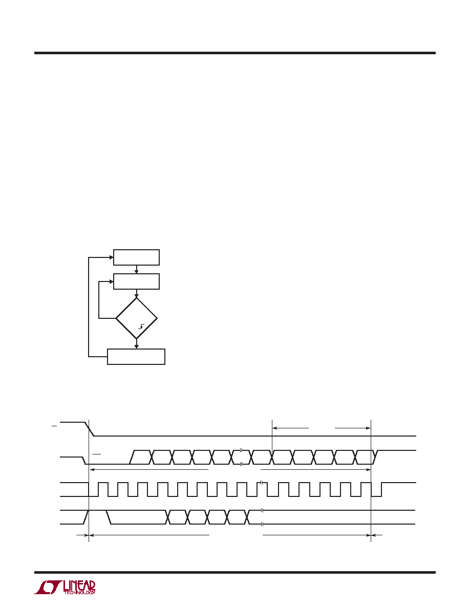
Converter Operation Cycle
The LTC2484 is a low power, delta-sigma analog-to-digital
converter with an easy to use 4-wire serial interface
and automatic differential input current cancellation.
Its operation is made up of three states. The converter
operating cycle begins with the conversion, followed by
the low power sleep state and ends with the data output
(see Figure 1). The 4-wire interface consists of serial data
output (SDO), serial clock (SCK), chip select (CS) and
serial data input (SDI).
Initially, the LTC2484 performs a conversion. Once the
conversion is complete, the device enters the sleep state.
CONVERT
SLEEP
DATA OUTPUT
CONFIGURATION INPUT
2484 F01
TRUE
FALSE
CS = LOW
AND
SCK
Figure 1. LTC2484 State Transition Diagram
CS
SDO
Hi-Z
SIG
DMY
BIT 29
MSB
CONVERSION RESULT
BIT 28
BIT 27
BIT 26
LSB24
BIT 4
BIT 5
BIT 3
BIT 1
BIT 0
BIT 2
BIT 30
SCK
SDI
SLEEP
DATA INPUT/OUTPUT
BIT 31
EOC
EN
DON’T CARE
IM
FOB
FOA
SPD
DON’T CARE
CONVERSION
2484 F02
SUB LSBs
Figure 2. Input/Output Data Timing
While in this sleep state, power consumption is
reduced by two orders of magnitude. The part re-
mains in the sleep state as long as CS is HIGH. The
conversion result is held indenitely in a static shift
register while the converter is in the sleep state.
Once CS is pulled LOW, the device exits the low
power mode and enters the data output state. If CS
is pulled HIGH before the rst rising edge of SCK,
the device returns to the low power sleep mode
and the conversion result is still held in the internal
static shift register. If CS remains LOW after the
rst rising edge of SCK, the device begins output-
ting the conversion result. Taking CS HIGH at this
point will terminate the data input and output state
and start a new conversion. The conversion result
is shifted out of the device through the serial data
output pin (SDO) on the falling edge of the serial
clock (SCK) (see Figure 2). The LTC2484 includes a
serial data input pin (SDI) in which data is latched
by the device on the rising edge of SCK (Figure 2).
The bit stream applied to this pin can be used to
select various features of the LTC2484, including an
on-chip temperature sensor, line frequency rejection
and output data rate. Alternatively, this pin may be
tied to ground and the part will perform conversions
in a default state. In the default state (SDI grounded)
the device simply performs conversions on the user
applied input with simultaneous rejection of 50Hz
and 60Hz line frequencies.
相关PDF资料 |
PDF描述 |
|---|---|
| LGU2W680MELY | CAP ALUM 68UF 450V 20% SNAP |
| EVAL-AD5516-1EBZ | BOARD EVAL FOR AD5516-1 2.5V |
| EBA22DRMN | CONN EDGECARD 44POS .125 SQ WW |
| SDR0302-330KL | INDUCTOR POWER 33UH 0.42A 0302 |
| EVAL-AD5516-2EBZ | BOARD EVALUATION FOR AD5516-2 |
相关代理商/技术参数 |
参数描述 |
|---|---|
| DC940KB-GB | 制造商:DEWALT 功能描述:DRILL 12V |
| DC941A | 功能描述:BOARD DELTA SIGMA ADC LTC2482 RoHS:是 类别:编程器,开发系统 >> 评估板 - 模数转换器 (ADC) 系列:Easy Drive™, QuikEval™ 产品培训模块:Obsolescence Mitigation Program 标准包装:1 系列:- ADC 的数量:1 位数:12 采样率(每秒):94.4k 数据接口:USB 输入范围:±VREF/2 在以下条件下的电源(标准):- 工作温度:-40°C ~ 85°C 已用 IC / 零件:MAX11645 已供物品:板,软件 |
| DC945KB | 制造商:DEWALT 功能描述:DRILL KIT CORDLESS 12V |
| DC945KB-GB | 制造商:DEWALT 功能描述:DRILL 12V |
| DC-9-500-2.1P | 制造商:SR COMPONENTS 功能描述: 制造商:SR Components Inc 功能描述: |
发布紧急采购,3分钟左右您将得到回复。