- 您现在的位置:买卖IC网 > PDF目录17123 > DK-DEV-4CGX150N (Altera)KIT DEVELOPMENT CYCLONE IV GX PDF资料下载
参数资料
| 型号: | DK-DEV-4CGX150N |
| 厂商: | Altera |
| 文件页数: | 20/42页 |
| 文件大小: | 0K |
| 描述: | KIT DEVELOPMENT CYCLONE IV GX |
| 应用说明: | Cyclone IV Design Guidelines |
| 产品培训模块: | Three Reasons to Use FPGA's in Industrial Designs Cyclone IV FPGA Family Overview |
| 软件下载: | DK-DEV-4CGX150N Kit Install |
| 特色产品: | Cyclone? IV GX FPGA Development Kit |
| 标准包装: | 1 |
| 系列: | CYCLONE® IV GX |
| 类型: | FPGA |
| 适用于相关产品: | Cyclone IV GX |
| 所含物品: | 板,线缆,文档,电源 |
| 其它名称: | 544-2713 |
第1页第2页第3页第4页第5页第6页第7页第8页第9页第10页第11页第12页第13页第14页第15页第16页第17页第18页第19页当前第20页第21页第22页第23页第24页第25页第26页第27页第28页第29页第30页第31页第32页第33页第34页第35页第36页第37页第38页第39页第40页第41页第42页
Chapter 1: Cyclone IV Device Datasheet
1–27
Switching Characteristics
December 2013
Altera Corporation
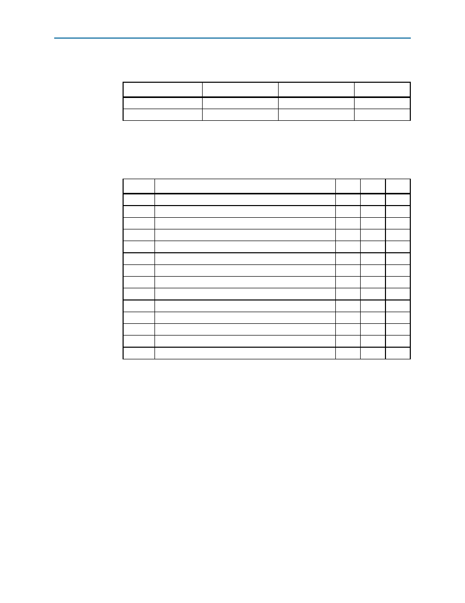
Table 1–29 lists the active configuration mode specifications for Cyclone IV devices.
Table 1–30 lists the JTAG timing parameters and values for Cyclone IV devices.
Periphery Performance
This section describes periphery performance, including high-speed I/O and external
memory interface.
I/O performance supports several system interfaces, such as the high-speed I/O
interface, external memory interface, and the PCI/PCI-X bus interface. I/Os using the
SSTL-18 Class I termination standard can achieve up to the stated DDR2 SDRAM
interfacing speeds. I/Os using general-purpose I/O standards such as 3.3-, 3.0-, 2.5-,
1.8-, or 1.5-LVTTL/LVCMOS are capable of a typical 200 MHz interfacing frequency
with a 10 pF load.
Table 1–29. Active Configuration Mode Specifications for Cyclone IV Devices
Programming Mode
DCLK Range
Typical DCLK
Unit
Active Parallel (AP) (1)
20 to 40
33
MHz
Active Serial (AS)
20 to 40
33
MHz
Note to Table 1–29:
(1) AP configuration mode is only supported for Cyclone IV E devices.
Table 1–30. JTAG Timing Parameters for Cyclone IV Devices (1)
Symbol
Parameter
Min
Max
Unit
tJCP
TCK clock period
40
—
ns
tJCH
TCK clock high time
19
—
ns
tJCL
TCK clock low time
19
—
ns
tJPSU_TDI
JTAG port setup time for TDI
1
—
ns
tJPSU_TMS JTAG port setup time for TMS
3
—
ns
tJPH
JTAG port hold time
10
—
ns
tJPCO
—15
ns
tJPZX
JTAG port high impedance to valid output (2), (3)
—15
ns
tJPXZ
JTAG port valid output to high impedance (2), (3)
—15
ns
tJSSU
Capture register setup time
5
—
ns
tJSH
Capture register hold time
10
—
ns
tJSCO
Update register clock to output
—
25
ns
tJSZX
Update register high impedance to valid output
—
25
ns
tJSXZ
Update register valid output to high impedance
—
25
ns
Notes to Table 1–30:
(1) For more information about JTAG waveforms, refer to “JTAG Waveform” in “Glossary” on page 1–37.
(2) The specification is shown for 3.3-, 3.0-, and 2.5-V LVTTL/LVCMOS operation of JTAG pins. For 1.8-V
LVTTL/LVCMOS and 1.5-V LVCMOS, the output time specification is 16 ns.
(3) For EP4CGX22, EP4CGX30 (F324 and smaller package), EP4CGX110, and EP4CGX150 devices, the output time
specification for 3.3-, 3.0-, and 2.5-V LVTTL/LVCMOS operation of JTAG pins is 16 ns. For 1.8-V LVTTL/LVCMOS
and 1.5-V LVCMOS, the output time specification is 18 ns.
相关PDF资料 |
PDF描述 |
|---|---|
| AIRD-02-2R7K | INDUCTOR PWR DRUM CORE 2.7UH |
| AIRD-02-1R5K | INDUCTOR PWR DRUM CORE 1.5UH |
| ECC30DJCB | CONN EDGECARD 60PS .100 PRESSFIT |
| D-SCE-1K-4.8-50-S1-9 | HEAT SHRINK SLEEVE MARKER |
| SPX1431S-L/TR | IC VREF SHUNT PREC ADJ 8-SOICN |
相关代理商/技术参数 |
参数描述 |
|---|---|
| DK-DEV-4CGX150N | 制造商:Altera Corporation 功能描述:KIT STARTER CYCLONE IV GX ((NS |
| DK-DEV-4S100G5N | 功能描述:可编程逻辑 IC 开发工具 FPGA Development Kit For EP4S100G5F RoHS:否 制造商:Altera Corporation 产品:Development Kits 类型:FPGA 工具用于评估:5CEFA7F3 接口类型: 工作电源电压: |
| DK-DEV-4SE530N | 功能描述:可编程逻辑 IC 开发工具 FPGA Development Kit For EP4SE530H35 RoHS:否 制造商:Altera Corporation 产品:Development Kits 类型:FPGA 工具用于评估:5CEFA7F3 接口类型: 工作电源电压: |
| DK-DEV-4SGX230N | 功能描述:可编程逻辑 IC 开发工具 FPGA Development Kit For EP4SGX230KF40C2N RoHS:否 制造商:Altera Corporation 产品:Development Kits 类型:FPGA 工具用于评估:5CEFA7F3 接口类型: 工作电源电压: |
| DK-DEV-4SGX230N/C2 | 功能描述:EP4SGX230KF40C2N Stratix? IV GX FPGA Evaluation Board 制造商:altera 系列:Stratix? IV GX 零件状态:过期 类型:FPGA 配套使用产品/相关产品:EP4SGX230KF40C2N 内容:板,线缆,电源 标准包装:1 |
发布紧急采购,3分钟左右您将得到回复。