- 您现在的位置:买卖IC网 > PDF目录17123 > DK-DEV-4CGX150N (Altera)KIT DEVELOPMENT CYCLONE IV GX PDF资料下载
参数资料
| 型号: | DK-DEV-4CGX150N |
| 厂商: | Altera |
| 文件页数: | 26/42页 |
| 文件大小: | 0K |
| 描述: | KIT DEVELOPMENT CYCLONE IV GX |
| 应用说明: | Cyclone IV Design Guidelines |
| 产品培训模块: | Three Reasons to Use FPGA's in Industrial Designs Cyclone IV FPGA Family Overview |
| 软件下载: | DK-DEV-4CGX150N Kit Install |
| 特色产品: | Cyclone? IV GX FPGA Development Kit |
| 标准包装: | 1 |
| 系列: | CYCLONE® IV GX |
| 类型: | FPGA |
| 适用于相关产品: | Cyclone IV GX |
| 所含物品: | 板,线缆,文档,电源 |
| 其它名称: | 544-2713 |
第1页第2页第3页第4页第5页第6页第7页第8页第9页第10页第11页第12页第13页第14页第15页第16页第17页第18页第19页第20页第21页第22页第23页第24页第25页当前第26页第27页第28页第29页第30页第31页第32页第33页第34页第35页第36页第37页第38页第39页第40页第41页第42页
1–32
Chapter 1: Cyclone IV Device Datasheet
Switching Characteristics
December 2013
Altera Corporation
External Memory Interface Specifications
The external memory interfaces for Cyclone IV devices are auto-calibrating and easy
to implement.
tDUTY
—
455545554555455545
55
%
TCCS
—
200
—
200
—
200
—
200
—
200
ps
Output jitter
(peak to peak)
—
500
—
500
—
550
—
600
—
700
ps
tLOCK (2)
—
1—
1
ms
Notes to Table 1–35:
(1) Cyclone IV E—emulated LVDS transmitter is supported at the output pin of all I/O Banks.
Cyclone IV GX—emulated LVDS transmitter is supported at the output pin of I/O Banks 3, 4, 5, 6, 7, 8, and 9.
(2) tLOCK is the time required for the PLL to lock from the end-of-device configuration.
(3) Cyclone IV E 1.0 V core voltage devices only support C8L, C9L, and I8L speed grades. Cyclone IV E 1.2 V core voltage devices only support
C6, C7, C8, I7, and A7 speed grades. Cyclone IV GX devices only support C6, C7, C8, and I7 speed grades.
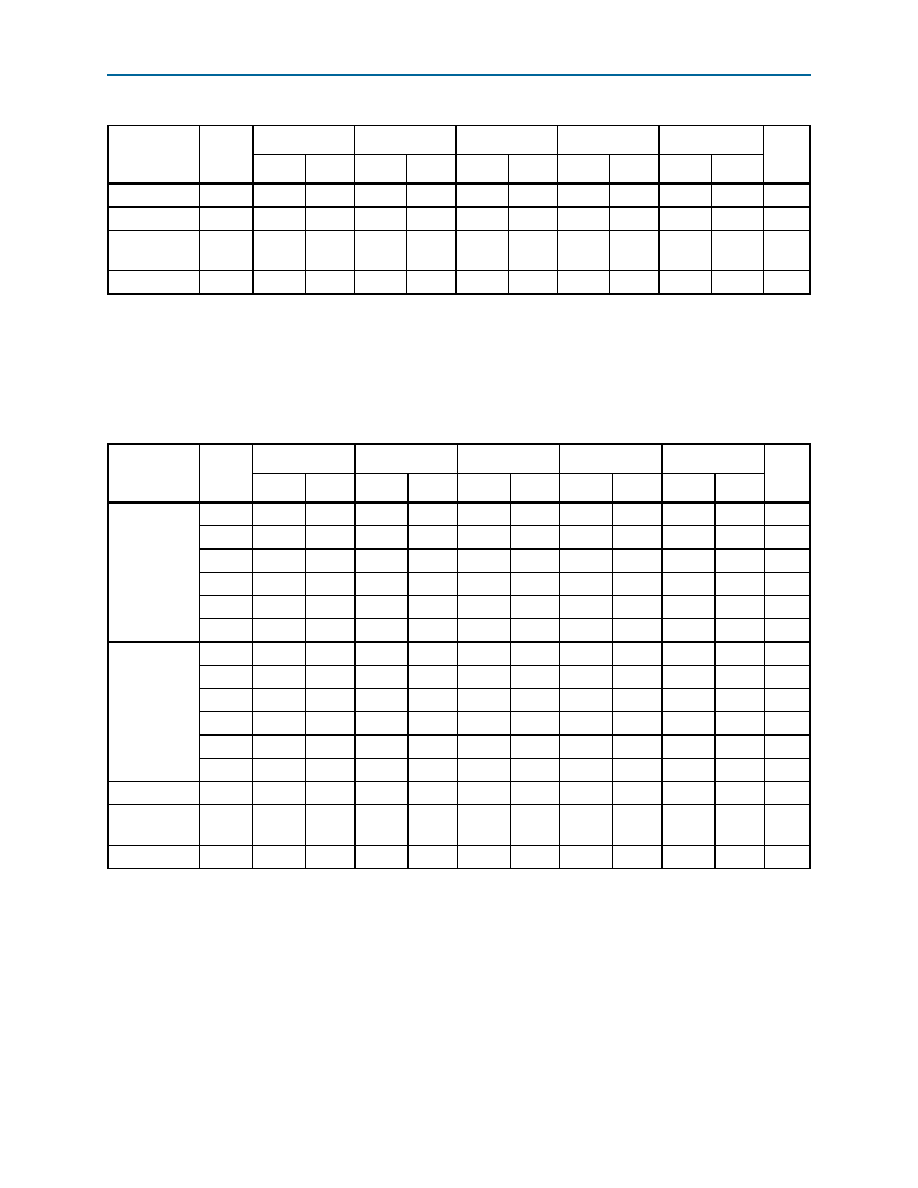
Table 1–35. Emulated LVDS Transmitter Timing Specifications for Cyclone IV Devices (1), (3) (Part 2 of 2)
Symbol
Modes
C6
C7, I7
C8, A7
C8L, I8L
C9L
Unit
Min
Max
Min
Max
Min
Max
Min
Max
Min
Max
Table 1–36. LVDS Receiver Timing Specifications for Cyclone IV Devices (1), (3)
Symbol
Modes
C6
C7, I7
C8, A7
C8L, I8L
C9L
Unit
Min
Max
Min
Max
Min
Max
Min
Max
Min
Max
fHSCLK (input
clock
frequency)
×10
10
437.5
10
370
10
320
10
320
10
250
MHz
×8
10
437.5
10
370
10
320
10
320
10
250
MHz
×7
10
437.5
10
370
10
320
10
320
10
250
MHz
×4
10
437.5
10
370
10
320
10
320
10
250
MHz
×2
10
437.5
10
370
10
320
10
320
10
250
MHz
×1
10
437.5
10
402.5
10
402.5
10
362
10
265
MHz
HSIODR
×10
100
875
100
740
100
640
100
640
100
500
Mbps
×8
80
875
80
740
80
640
80
640
80
500
Mbps
×7
70
875
70
740
70
640
70
640
70
500
Mbps
×4
40
875
40
740
40
640
40
640
40
500
Mbps
×2
20
875
20
740
20
640
20
640
20
500
Mbps
×1
10
437.5
10
402.5
10
402.5
10
362
10
265
Mbps
SW
—
400
—
400
—
400
—
550
—
640
ps
Input jitter
tolerance
—
500
—
500
—
550
—
600
—
700
ps
tLOCK (2)
—
—1—1—1—1—
1
ms
Notes to Table 1–36:
(1) Cyclone IV E—LVDS receiver is supported at all I/O Banks.
Cyclone IV GX—LVDS receiver is supported at I/O Banks 3, 4, 5, 6, 7, 8, and 9.
(2) tLOCK is the time required for the PLL to lock from the end-of-device configuration.
(3) Cyclone IV E 1.0 V core voltage devices only support C8L, C9L, and I8L speed grades. Cyclone IV E 1.2 V core voltage devices only support
C6, C7, C8, I7, and A7 speed grades. Cyclone IV GX devices only support C6, C7, C8, and I7 speed grades.
相关PDF资料 |
PDF描述 |
|---|---|
| AIRD-02-2R7K | INDUCTOR PWR DRUM CORE 2.7UH |
| AIRD-02-1R5K | INDUCTOR PWR DRUM CORE 1.5UH |
| ECC30DJCB | CONN EDGECARD 60PS .100 PRESSFIT |
| D-SCE-1K-4.8-50-S1-9 | HEAT SHRINK SLEEVE MARKER |
| SPX1431S-L/TR | IC VREF SHUNT PREC ADJ 8-SOICN |
相关代理商/技术参数 |
参数描述 |
|---|---|
| DK-DEV-4CGX150N | 制造商:Altera Corporation 功能描述:KIT STARTER CYCLONE IV GX ((NS |
| DK-DEV-4S100G5N | 功能描述:可编程逻辑 IC 开发工具 FPGA Development Kit For EP4S100G5F RoHS:否 制造商:Altera Corporation 产品:Development Kits 类型:FPGA 工具用于评估:5CEFA7F3 接口类型: 工作电源电压: |
| DK-DEV-4SE530N | 功能描述:可编程逻辑 IC 开发工具 FPGA Development Kit For EP4SE530H35 RoHS:否 制造商:Altera Corporation 产品:Development Kits 类型:FPGA 工具用于评估:5CEFA7F3 接口类型: 工作电源电压: |
| DK-DEV-4SGX230N | 功能描述:可编程逻辑 IC 开发工具 FPGA Development Kit For EP4SGX230KF40C2N RoHS:否 制造商:Altera Corporation 产品:Development Kits 类型:FPGA 工具用于评估:5CEFA7F3 接口类型: 工作电源电压: |
| DK-DEV-4SGX230N/C2 | 功能描述:EP4SGX230KF40C2N Stratix? IV GX FPGA Evaluation Board 制造商:altera 系列:Stratix? IV GX 零件状态:过期 类型:FPGA 配套使用产品/相关产品:EP4SGX230KF40C2N 内容:板,线缆,电源 标准包装:1 |
发布紧急采购,3分钟左右您将得到回复。