- 您现在的位置:买卖IC网 > PDF目录17123 > DK-DEV-4CGX150N (Altera)KIT DEVELOPMENT CYCLONE IV GX PDF资料下载
参数资料
| 型号: | DK-DEV-4CGX150N |
| 厂商: | Altera |
| 文件页数: | 35/42页 |
| 文件大小: | 0K |
| 描述: | KIT DEVELOPMENT CYCLONE IV GX |
| 应用说明: | Cyclone IV Design Guidelines |
| 产品培训模块: | Three Reasons to Use FPGA's in Industrial Designs Cyclone IV FPGA Family Overview |
| 软件下载: | DK-DEV-4CGX150N Kit Install |
| 特色产品: | Cyclone? IV GX FPGA Development Kit |
| 标准包装: | 1 |
| 系列: | CYCLONE® IV GX |
| 类型: | FPGA |
| 适用于相关产品: | Cyclone IV GX |
| 所含物品: | 板,线缆,文档,电源 |
| 其它名称: | 544-2713 |
第1页第2页第3页第4页第5页第6页第7页第8页第9页第10页第11页第12页第13页第14页第15页第16页第17页第18页第19页第20页第21页第22页第23页第24页第25页第26页第27页第28页第29页第30页第31页第32页第33页第34页当前第35页第36页第37页第38页第39页第40页第41页第42页
1–40
Chapter 1: Cyclone IV Device Datasheet
Glossary
December 2013
Altera Corporation
T
tC
High-speed receiver and transmitter input and output clock period.
Channel-to-
channel-skew
(TCCS)
High-speed I/O block: The timing difference between the fastest and slowest output edges,
including tCO variation and clock skew. The clock is included in the TCCS measurement.
tcin
Delay from the clock pad to the I/O input register.
tCO
Delay from the clock pad to the I/O output.
tcout
Delay from the clock pad to the I/O output register.
tDUTY
High-speed I/O block: Duty cycle on high-speed transmitter output clock.
tFALL
Signal high-to-low transition time (80–20%).
tH
Input register hold time.
Timing Unit
Interval (TUI)
High-speed I/O block: The timing budget allowed for skew, propagation delays, and data
sampling window. (TUI = 1/(Receiver Input Clock Frequency Multiplication Factor) = tC/w).
tINJITTER
Period jitter on the PLL clock input.
tOUTJITTER_DEDCLK
Period jitter on the dedicated clock output driven by a PLL.
tOUTJITTER_IO
Period jitter on the general purpose I/O driven by a PLL.
tpllcin
Delay from the PLL inclk pad to the I/O input register.
tpllcout
Delay from the PLL inclk pad to the I/O output register.
Transmitter
Output
Waveform
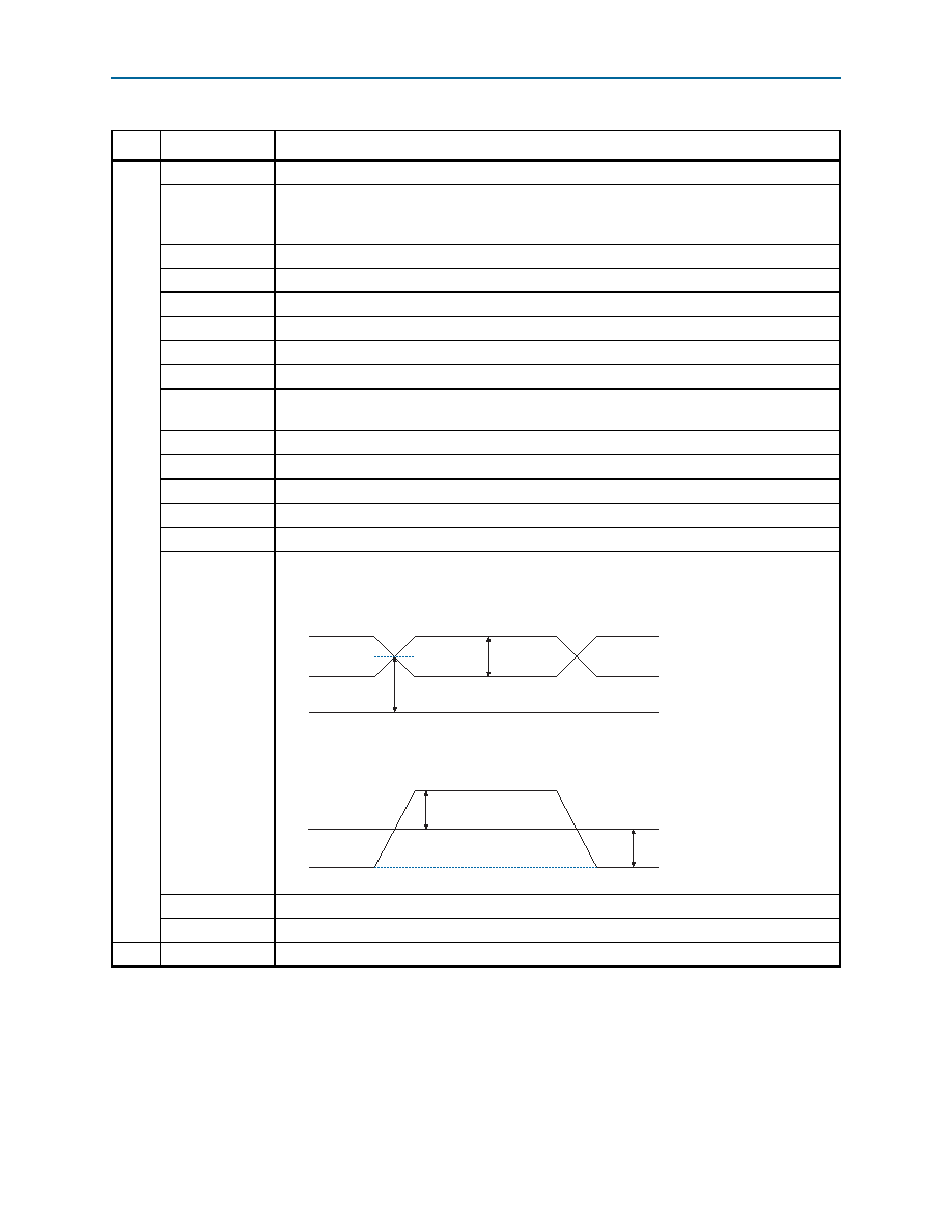
Transmitter output waveforms for the LVDS, mini-LVDS, PPDS and RSDS Differential I/O
Standards:
tRISE
Signal low-to-high transition time (20–80%).
tSU
Input register setup time.
U
——
Table 1–46. Glossary (Part 4 of 5)
Letter
Term
Definitions
Single-Ended Waveform
Differential Waveform (Mathematical Function of Positive & Negative Channel)
Positive Channel (p) = V
OH
Negative Channel (n) = V
OL
Ground
VOD
V
OD
V
OD
0 V
Vos
p
- n
相关PDF资料 |
PDF描述 |
|---|---|
| AIRD-02-2R7K | INDUCTOR PWR DRUM CORE 2.7UH |
| AIRD-02-1R5K | INDUCTOR PWR DRUM CORE 1.5UH |
| ECC30DJCB | CONN EDGECARD 60PS .100 PRESSFIT |
| D-SCE-1K-4.8-50-S1-9 | HEAT SHRINK SLEEVE MARKER |
| SPX1431S-L/TR | IC VREF SHUNT PREC ADJ 8-SOICN |
相关代理商/技术参数 |
参数描述 |
|---|---|
| DK-DEV-4CGX150N | 制造商:Altera Corporation 功能描述:KIT STARTER CYCLONE IV GX ((NS |
| DK-DEV-4S100G5N | 功能描述:可编程逻辑 IC 开发工具 FPGA Development Kit For EP4S100G5F RoHS:否 制造商:Altera Corporation 产品:Development Kits 类型:FPGA 工具用于评估:5CEFA7F3 接口类型: 工作电源电压: |
| DK-DEV-4SE530N | 功能描述:可编程逻辑 IC 开发工具 FPGA Development Kit For EP4SE530H35 RoHS:否 制造商:Altera Corporation 产品:Development Kits 类型:FPGA 工具用于评估:5CEFA7F3 接口类型: 工作电源电压: |
| DK-DEV-4SGX230N | 功能描述:可编程逻辑 IC 开发工具 FPGA Development Kit For EP4SGX230KF40C2N RoHS:否 制造商:Altera Corporation 产品:Development Kits 类型:FPGA 工具用于评估:5CEFA7F3 接口类型: 工作电源电压: |
| DK-DEV-4SGX230N/C2 | 功能描述:EP4SGX230KF40C2N Stratix? IV GX FPGA Evaluation Board 制造商:altera 系列:Stratix? IV GX 零件状态:过期 类型:FPGA 配套使用产品/相关产品:EP4SGX230KF40C2N 内容:板,线缆,电源 标准包装:1 |
发布紧急采购,3分钟左右您将得到回复。