- 您现在的位置:买卖IC网 > PDF目录10491 > DS21448L+ (Maxim Integrated Products)IC LIU QUAD E1/T1/J1 128-LQFP PDF资料下载
参数资料
| 型号: | DS21448L+ |
| 厂商: | Maxim Integrated Products |
| 文件页数: | 16/60页 |
| 文件大小: | 0K |
| 描述: | IC LIU QUAD E1/T1/J1 128-LQFP |
| 产品培训模块: | Lead (SnPb) Finish for COTS Obsolescence Mitigation Program |
| 标准包装: | 72 |
| 类型: | 线路接口装置(LIU) |
| 驱动器/接收器数: | 4/4 |
| 规程: | T1/E1/J1 |
| 电源电压: | 3.135 V ~ 3.465 V |
| 安装类型: | 表面贴装 |
| 封装/外壳: | 128-LQFP |
| 供应商设备封装: | 128-LQFP(14x20) |
| 包装: | 管件 |
| 产品目录页面: | 1430 (CN2011-ZH PDF) |
第1页第2页第3页第4页第5页第6页第7页第8页第9页第10页第11页第12页第13页第14页第15页当前第16页第17页第18页第19页第20页第21页第22页第23页第24页第25页第26页第27页第28页第29页第30页第31页第32页第33页第34页第35页第36页第37页第38页第39页第40页第41页第42页第43页第44页第45页第46页第47页第48页第49页第50页第51页第52页第53页第54页第55页第56页第57页第58页第59页第60页
DS21448 3.3V T1/E1/J1 Quad Line Interface
23 of 60
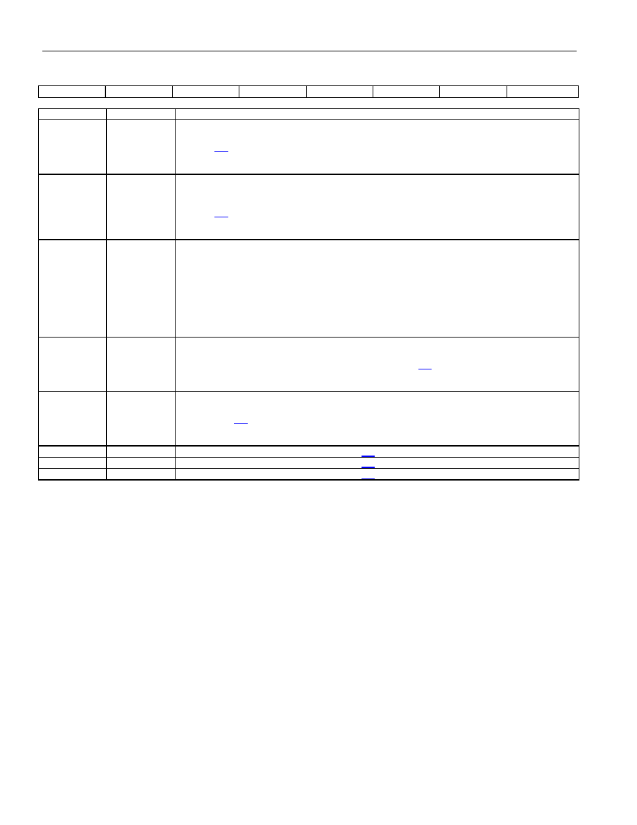
CCR6 (05H): Common Control Register 6
(MSB)
(LSB)
LLB
RLB
ARLBE
ALB
RJAB
ECRS2
ECRS1
ECRS0
NAME
POSITION
FUNCTION
LLB
CCR6.7
Local Loopback. In local loopback, transmit data is looped back to the receive path, passing
through the jitter attenuator if it is enabled. Data in the transmit path acts as normal. See
Section 6.2 for details.
0 = loopback disabled
1 = loopback enabled
RLB
CCR6.6
Remote Loopback. In remote loopback, data output from the clock/data recovery circuitry is
looped back to the transmit path, passing through the jitter attenuator if it is enabled. Data in
the receive path acts as normal, while data presented at TPOS and TNEG is ignored. See
Section 6.2 for details.
0 = loopback disabled
1 = loopback enabled
ARLBE
CCR6.5
Automatic Remote Loopback Enable and Reset. When this bit is set high, the device
automatically goes into remote loopback when it detects loop-up code programmed into the
receive loop-up code definition registers (RUPCD1 and RUPCD2) for a minimum of 5
seconds; it also sets the RIR2.1 status bit. Once it is in an RLB state, the bit remains in this
state until it has detected the loop code programmed into the receive loop-down code
definition registers (RDNCD1 and RDNCD2) for a minimum of 5 seconds, at which point it
forces the device out of RLB and clears RIR2.1. Toggling this bit from 1 to 0 resets the
automatic RLB circuitry. The action of the automatic remote loopback circuitry is logically
ORed with the RLB (CCR6.6) control bit (i.e., either one can cause a RLB to occur).
ALB
CCR6.4
Analog Loopback. In analog loopback, signals at TTIP and TRING are internally connected to
RTIP and RRING. The incoming line signals at RTIP and RRING are ignored. The signals at
TTIP and TRING are transmitted as normal. See Section 6.2 for more details.
0 = loopback disabled
1 = loopback enabled
RJAB
CCR6.3
RCLK Jitter Attenuator Bypass. This control bit allows the receive-recovered clock and data to
bypass the jitter attenuation, while still allowing the BPCLK output to use the jitter attenuator.
See Section 7.3 for details.
0 = disabled
1 = enabled
ECRS2
CCR6.2
Error Count Register Select 2. See Section 6.4 for details.
ECRS1
CCR6.1
Error Count Register Select 1. See Section 6.4 for details.
ECRS0
CCR6.0
Error Count Register Select 0. See Section 6.4 for details.
5. STATUS REGISTERS
The three registers that contain information about the device’s real-time status are the status register (SR) and
receive information registers 1 and 2 (RIR1/RIR2). When a particular event has occurred (or is occurring), the
appropriate bit in one of these registers is set to 1. Some bits in SR, RIR1, and RIR2 are latched bits and some are
real-time bits (denoted in the following register descriptions). For latched status bits, when an event or an alarm
occurs, the bit is set to 1 and remains set until the user reads that bit. The bit is cleared when it is read, and it is not
set until the event has occurred again. Two of the latched status bits (RUA1 and RCL) remain set after reading if
the alarm is still present.
The user always precedes a read of any of the three status registers with a write. The byte written to the register
informs the DS21448 which bits the user wishes to read and have cleared. The user writes a byte to one of these
registers with a 1 in the bit positions to be read and a 0 in the other bit positions. When a 1 is written to a bit
location, that location is updated with the latest information. When a 0 is written to a bit position, that bit position is
not updated, and the previous value is held. A write to the status and information registers is immediately followed
by a read of the same register. The read result should be logically ANDed with the mask byte that was just written,
and this value should be written back into the same register to ensure that bit does indeed clear. This second write
step is necessary because the alarms and events in the status registers occur asynchronously with respect to their
access through the parallel port. This write-read-write scheme allows an external microcontroller or microprocessor
to individually poll certain bits without disturbing the other bits in the register. This operation is key in controlling the
DS21448 with higher-order software languages.
相关PDF资料 |
PDF描述 |
|---|---|
| VI-2T1-IV-B1 | CONVERTER MOD DC/DC 12V 150W |
| FAN3850AUC16X | IC MICROPHONE PRE-AMP 6-WLCSP |
| MAX1296AEEG+ | IC ADC 12BIT 420KSPS 24-QSOP |
| UP050SL110J-KFC | CAP CER 11PF 50V 5% AXIAL |
| VI-2T0-IV-B1 | CONVERTER MOD DC/DC 5V 150W |
相关代理商/技术参数 |
参数描述 |
|---|---|
| DS21448L+ | 功能描述:网络控制器与处理器 IC 3.3V E1/T1/J1 Quad Interface RoHS:否 制造商:Micrel 产品:Controller Area Network (CAN) 收发器数量: 数据速率: 电源电流(最大值):595 mA 最大工作温度:+ 85 C 安装风格:SMD/SMT 封装 / 箱体:PBGA-400 封装:Tray |
| DS21448L+W | 功能描述:网络控制器与处理器 IC 3.3V E1/T1/J1 Quad Interface RoHS:否 制造商:Micrel 产品:Controller Area Network (CAN) 收发器数量: 数据速率: 电源电流(最大值):595 mA 最大工作温度:+ 85 C 安装风格:SMD/SMT 封装 / 箱体:PBGA-400 封装:Tray |
| DS21448LDK | 功能描述:KIT DESIGN LIU DS21448L T1/J1/E1 RoHS:否 类别:编程器,开发系统 >> 过时/停产零件编号 系列:- 标准包装:1 系列:- 传感器类型:CMOS 成像,彩色(RGB) 传感范围:WVGA 接口:I²C 灵敏度:60 fps 电源电压:5.7 V ~ 6.3 V 嵌入式:否 已供物品:成像器板 已用 IC / 零件:KAC-00401 相关产品:4H2099-ND - SENSOR IMAGE WVGA COLOR 48-PQFP4H2094-ND - SENSOR IMAGE WVGA MONO 48-PQFP |
| DS21448LN | 功能描述:网络控制器与处理器 IC 3.3V E1/T1/J1 Quad Interface RoHS:否 制造商:Micrel 产品:Controller Area Network (CAN) 收发器数量: 数据速率: 电源电流(最大值):595 mA 最大工作温度:+ 85 C 安装风格:SMD/SMT 封装 / 箱体:PBGA-400 封装:Tray |
| DS21448LN+ | 功能描述:网络控制器与处理器 IC 3.3V E1/T1/J1 Quad Interface RoHS:否 制造商:Micrel 产品:Controller Area Network (CAN) 收发器数量: 数据速率: 电源电流(最大值):595 mA 最大工作温度:+ 85 C 安装风格:SMD/SMT 封装 / 箱体:PBGA-400 封装:Tray |
发布紧急采购,3分钟左右您将得到回复。