- 您现在的位置:买卖IC网 > PDF目录10491 > DS21448L+ (Maxim Integrated Products)IC LIU QUAD E1/T1/J1 128-LQFP PDF资料下载
参数资料
| 型号: | DS21448L+ |
| 厂商: | Maxim Integrated Products |
| 文件页数: | 7/60页 |
| 文件大小: | 0K |
| 描述: | IC LIU QUAD E1/T1/J1 128-LQFP |
| 产品培训模块: | Lead (SnPb) Finish for COTS Obsolescence Mitigation Program |
| 标准包装: | 72 |
| 类型: | 线路接口装置(LIU) |
| 驱动器/接收器数: | 4/4 |
| 规程: | T1/E1/J1 |
| 电源电压: | 3.135 V ~ 3.465 V |
| 安装类型: | 表面贴装 |
| 封装/外壳: | 128-LQFP |
| 供应商设备封装: | 128-LQFP(14x20) |
| 包装: | 管件 |
| 产品目录页面: | 1430 (CN2011-ZH PDF) |
第1页第2页第3页第4页第5页第6页当前第7页第8页第9页第10页第11页第12页第13页第14页第15页第16页第17页第18页第19页第20页第21页第22页第23页第24页第25页第26页第27页第28页第29页第30页第31页第32页第33页第34页第35页第36页第37页第38页第39页第40页第41页第42页第43页第44页第45页第46页第47页第48页第49页第50页第51页第52页第53页第54页第55页第56页第57页第58页第59页第60页
DS21448 3.3V T1/E1/J1 Quad Line Interface
15 of 60
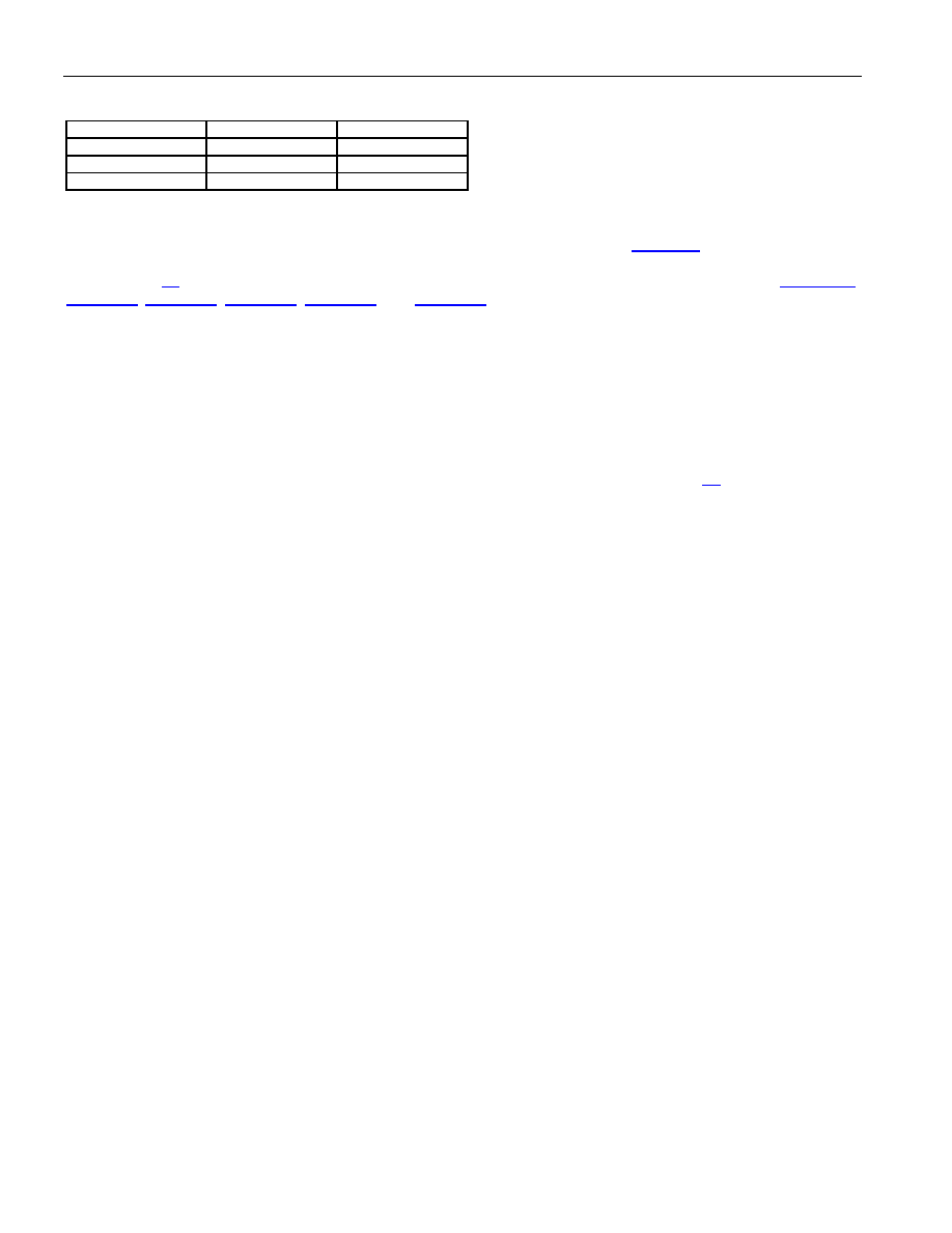
Table 4-F. MCLK Selection in Hardware Mode
MCLK (MHz)
JAMUX
ETS
2.048
0
2.048
1
1.544
0
1
4.2 Serial Port Operation
Setting BIS1 = 1 and BIS0 = 0 enables the serial bus interface on the DS21448 (Table 2-A). Serial port read/write
timing is unrelated to the system transmit and receive timing, allowing asynchronous reads or writes by the host.
See Section 10 for the AC timing of the serial port. All serial port accesses are LSB first. See Figure 4-1,
A serial bus access requires the use of four signals: serial clock (SCLK), one of the four chip selects (
CS), serial
data input (SDI), and serial data output (SDO). The DS21448 uses SCLK to sample data that is present on SDI and
output data onto SDO. Input clock-edge select (ICES) allows the user to choose which SCLK edge input data is
sampled on. Output clock-edge select (OCES) allows the user to choose which SCLK edge output data changes
on. When ICES is low, input data is latched on the rising edge of SCLK, and when ICES is high, input data is
latched on the falling edge of SCLK. When OCES is low, data is output on the falling edge of SCLK, and when
OCES is high, data is output on the rising edge of SCLK. Data is held until the next falling or rising edge of SCLK.
All data transfers are initiated by driving the appropriate port’s
CS input low and ends with CS going inactive. CS
must go inactive between data transfers. See the serial bus timing information in Section 10 for details. All data
transfers are terminated if the port’s
CS input transitions high. Port control logic is disabled, and SDO is tri-stated
when all
CS pins are inactive.
Reading from or writing to the internal registers requires writing one address/command byte prior to the transferring
register data. Two types of serial bus transfers exist, standard and burst. The standard serial bus access always
consists of two bytes, an address/command byte that is always supplied by the user on SDI, and a data byte that
can either be written to the DS21448 using SDI (write operation) or output by the DS21448 on SDO (read
operation). The burst serial bus access consists of a single address/command byte followed either by 22 read or 22
write data bytes.
The first bit written (LSB) of the address/command byte specifies whether the access is to be a read (1) or a write
(0). The next 5 bits identify the register address. Valid register addresses are 00h through 15h. Bit 7 is reserved
and must be set to 0 for proper operation. Bit 8, the last bit (MSB) of the address/command byte, is the burst mode-
enable bit. When the burst bit is enabled (set to 0) and a READ operation is performed, the DS21448 automatically
outputs the contents of registers 00h through 15h sequentially, starting with register address 00h. When the burst
bit is enabled and a WRITE operation is performed, data supplied on SDI is sequentially written into the DS21448’s
register space starting at address 00h. Burst operation is stopped once address 15h is read or
CS goes inactive.
For both burst read and burst write transfers, the address/command byte’s register address bits must be set to 0.
The user can broadcast register write accesses to multiple ports simultaneously by enabling the desired channels’
chip selects at the same time. However, only one port can be read at a time. Any attempt to read multiple ports
simultaneously results in invalid data being returned on SDO.
相关PDF资料 |
PDF描述 |
|---|---|
| VI-2T1-IV-B1 | CONVERTER MOD DC/DC 12V 150W |
| FAN3850AUC16X | IC MICROPHONE PRE-AMP 6-WLCSP |
| MAX1296AEEG+ | IC ADC 12BIT 420KSPS 24-QSOP |
| UP050SL110J-KFC | CAP CER 11PF 50V 5% AXIAL |
| VI-2T0-IV-B1 | CONVERTER MOD DC/DC 5V 150W |
相关代理商/技术参数 |
参数描述 |
|---|---|
| DS21448L+ | 功能描述:网络控制器与处理器 IC 3.3V E1/T1/J1 Quad Interface RoHS:否 制造商:Micrel 产品:Controller Area Network (CAN) 收发器数量: 数据速率: 电源电流(最大值):595 mA 最大工作温度:+ 85 C 安装风格:SMD/SMT 封装 / 箱体:PBGA-400 封装:Tray |
| DS21448L+W | 功能描述:网络控制器与处理器 IC 3.3V E1/T1/J1 Quad Interface RoHS:否 制造商:Micrel 产品:Controller Area Network (CAN) 收发器数量: 数据速率: 电源电流(最大值):595 mA 最大工作温度:+ 85 C 安装风格:SMD/SMT 封装 / 箱体:PBGA-400 封装:Tray |
| DS21448LDK | 功能描述:KIT DESIGN LIU DS21448L T1/J1/E1 RoHS:否 类别:编程器,开发系统 >> 过时/停产零件编号 系列:- 标准包装:1 系列:- 传感器类型:CMOS 成像,彩色(RGB) 传感范围:WVGA 接口:I²C 灵敏度:60 fps 电源电压:5.7 V ~ 6.3 V 嵌入式:否 已供物品:成像器板 已用 IC / 零件:KAC-00401 相关产品:4H2099-ND - SENSOR IMAGE WVGA COLOR 48-PQFP4H2094-ND - SENSOR IMAGE WVGA MONO 48-PQFP |
| DS21448LN | 功能描述:网络控制器与处理器 IC 3.3V E1/T1/J1 Quad Interface RoHS:否 制造商:Micrel 产品:Controller Area Network (CAN) 收发器数量: 数据速率: 电源电流(最大值):595 mA 最大工作温度:+ 85 C 安装风格:SMD/SMT 封装 / 箱体:PBGA-400 封装:Tray |
| DS21448LN+ | 功能描述:网络控制器与处理器 IC 3.3V E1/T1/J1 Quad Interface RoHS:否 制造商:Micrel 产品:Controller Area Network (CAN) 收发器数量: 数据速率: 电源电流(最大值):595 mA 最大工作温度:+ 85 C 安装风格:SMD/SMT 封装 / 箱体:PBGA-400 封装:Tray |
发布紧急采购,3分钟左右您将得到回复。