- 您现在的位置:买卖IC网 > PDF目录1914 > DS21Q50LN (Maxim Integrated Products)IC TRANSCEIVER E1 QD IND 100LQFP PDF资料下载
参数资料
| 型号: | DS21Q50LN |
| 厂商: | Maxim Integrated Products |
| 文件页数: | 41/87页 |
| 文件大小: | 0K |
| 描述: | IC TRANSCEIVER E1 QD IND 100LQFP |
| 产品培训模块: | Lead (SnPb) Finish for COTS |
| 产品变化通告: | Product Discontinuation 20/Feb/2012 |
| 标准包装: | 90 |
| 功能: | 收发器 |
| 接口: | E1 |
| 电路数: | 4 |
| 电源电压: | 3.14 V ~ 3.47 V |
| 电流 - 电源: | 230mA |
| 工作温度: | -40°C ~ 85°C |
| 安装类型: | 表面贴装 |
| 封装/外壳: | 100-LQFP |
| 供应商设备封装: | 100-LQFP(14x14) |
| 包装: | 托盘 |
| 包括: | AIS 警报检测器和发生器,回送功能,PRBS 发生器 / 检测器,远程检测器和发生器 |
第1页第2页第3页第4页第5页第6页第7页第8页第9页第10页第11页第12页第13页第14页第15页第16页第17页第18页第19页第20页第21页第22页第23页第24页第25页第26页第27页第28页第29页第30页第31页第32页第33页第34页第35页第36页第37页第38页第39页第40页当前第41页第42页第43页第44页第45页第46页第47页第48页第49页第50页第51页第52页第53页第54页第55页第56页第57页第58页第59页第60页第61页第62页第63页第64页第65页第66页第67页第68页第69页第70页第71页第72页第73页第74页第75页第76页第77页第78页第79页第80页第81页第82页第83页第84页第85页第86页第87页
DS21Q50
46 of 87
9. SYSTEM CLOCK INTERFACE
A single system clock interface (SCI) is common to the four DS21Q50 transceivers. The SCI allows any
one of the four receivers to act as the master reference clock for the system. When multiple DS21Q50s
are used to build an N port system, the SCI allows any one of the N ports to be the master. The selected
reference is then distributed to the other DS21Q50s through the REFCLK pin. The REFCLK pin acts as
an output on the DS21Q50, which has been selected to provide the reference clock from one of its four
receivers. On DS21Q50s not selected to source the reference clock, this pin becomes an input by writing
0s to the SCSx bits. The reference clock is also passed to the clock synthesizer PLL to generate a
2.048MHz, 4.096MHz, 8.192MHz, or 16.384MHz clock. This clock can then be used with the IBO
function to merge up to eight E1 lines onto a single high-speed PCM bus. If the master E1 port fails
(enters a receive carrier-loss condition), that port automatically switches to the clock present on the
MCLK pin. Therefore, MCLK acts as the backup source of master clock. The host can then find and
select a functioning E1 port as the master. Because the selected port’s clock is passed to the other
DS21Q50s in a multiple device configuration, one DS21Q50’s synthesizer can always be the source of
the high-speed clock. This allows smooth transitions when clock-source switching occurs. The SCI
control register exists in transceiver 1 only (TS0, TS1 = 0).
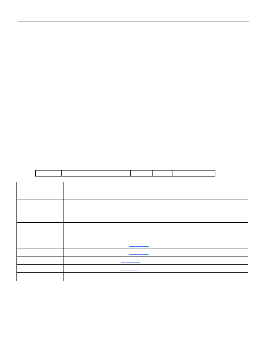
Register Name:
SCICR
Register Description:
System Clock Interface Control Register (Note: This register is valid
only for transceiver 1 (TS0 = 0, TS1 = 0).
Register Address:
1D Hex
Bit
7
6
5
4
3
2
1
0
Name
AJACKE
BUCS
SOE
CSS1
CSS0
SCS2
SCS1
SCS0
NAME
BIT
FUNCTION
AJACKE
7
AJACK Enable. This bit enables the alternate jitter attenuator.
BUCS
6
Backup Clock Select. Selects which clock source to switch to automatically during a loss-
of-transmit clock event.
0 = During an LOTC event, switch to MCLK
1 = During an LOTC event, switch to system reference clock
SOE
5
Synthesizer Output Enable
0 = 2/4/8/16MCK pin in high-Z mode
1 = 2/4/8/16MCK pin active
CSS1
4
Clock Synthesizer Select Bit 1 (Table 9-2)
CSS0
3
Clock Synthesizer Select Bit 0 (Table 9-2)
SCS2
2
System Clock Select Bit 2 (Table 9-1)
SCS1
1
System Clock Select Bit 1 (Table 9-1)
SCS0
0
System Clock Select Bit 0 (Table 9-1)
相关PDF资料 |
PDF描述 |
|---|---|
| DS21Q55 | IC TXRX QUAD T1/E1/J1 SCT 256BGA |
| DS21Q59LN+ | IC TXRX E1 QUAD 100-LQFP |
| DS21S07AS+T&R | IC TERMINATOR SCSI 16-SOIC |
| DS21T05Z/T&R | IC TERMINATOR SCSI 150MIL 16SOIC |
| DS21T07S+T&R | IC TERMINATOR SCSI 16-SOIC |
相关代理商/技术参数 |
参数描述 |
|---|---|
| DS21Q50LN+ | 功能描述:网络控制器与处理器 IC Quad E1 Transceiver RoHS:否 制造商:Micrel 产品:Controller Area Network (CAN) 收发器数量: 数据速率: 电源电流(最大值):595 mA 最大工作温度:+ 85 C 安装风格:SMD/SMT 封装 / 箱体:PBGA-400 封装:Tray |
| DS21Q50L-W+ | 功能描述:网络控制器与处理器 IC Quad E1 Transceiver RoHS:否 制造商:Micrel 产品:Controller Area Network (CAN) 收发器数量: 数据速率: 电源电流(最大值):595 mA 最大工作温度:+ 85 C 安装风格:SMD/SMT 封装 / 箱体:PBGA-400 封装:Tray |
| DS21Q50N | 制造商:未知厂家 制造商全称:未知厂家 功能描述:Telecommunication IC |
| DS21Q55 | 功能描述:IC TXRX QUAD T1/E1/J1 SCT 256BGA RoHS:否 类别:集成电路 (IC) >> 接口 - 电信 系列:- 产品培训模块:Lead (SnPb) Finish for COTS 产品变化通告:Product Discontinuation 06/Feb/2012 标准包装:750 系列:* |
| DS21Q552 | 功能描述:网络控制器与处理器 IC 5V Quad T1 Transceiver RoHS:否 制造商:Micrel 产品:Controller Area Network (CAN) 收发器数量: 数据速率: 电源电流(最大值):595 mA 最大工作温度:+ 85 C 安装风格:SMD/SMT 封装 / 箱体:PBGA-400 封装:Tray |
发布紧急采购,3分钟左右您将得到回复。