参数资料
| 型号: | DS3106DK |
| 厂商: | Maxim Integrated Products |
| 文件页数: | 10/32页 |
| 文件大小: | 0K |
| 描述: | KIT DEMO FOR DS3106 |
| 产品培训模块: | Lead (SnPb) Finish for COTS Obsolescence Mitigation Program |
| 标准包装: | 1 |
| 主要目的: | 计时,线路卡 |
| 已用 IC / 零件: | DS3106 |
| 已供物品: | 板,CD |
第1页第2页第3页第4页第5页第6页第7页第8页第9页当前第10页第11页第12页第13页第14页第15页第16页第17页第18页第19页第20页第21页第22页第23页第24页第25页第26页第27页第28页第29页第30页第31页第32页
�� �
�
�_________________________________________________________________________________________DS3106DK�
�4.4�
�T0� APLL� and� T0� APLL2�
�The� Input� Freq� field� configures� the� frequency� of� the� T0� APLL� DFS� (refer� to� the� DS3106� data� sheet� for� details).� The�
�APLL� output� frequency� is� always� four� times� the� input� frequency.� When� the� Input� Freq� field� is� changed,� the� Output�
�Freq� field� changes� to� match,� and� all� the� T0� options� in� the� OC3� and� OC6� output� clock� combo� boxes� also� change� to�
�frequencies� derived� from� the� new� T0� APLL� frequency.� These� changes� match� what� happens� in� the� DS3106.�
�In� normal� operation� the� T0� APLL2� has� a� fixed� output� frequency� of� 312.5MHz� (twice� the� standard� XGMII� clock� rate).�
�The� rate� is� displayed� in� the� T0� APLL2� Output� Freq� text� box.�
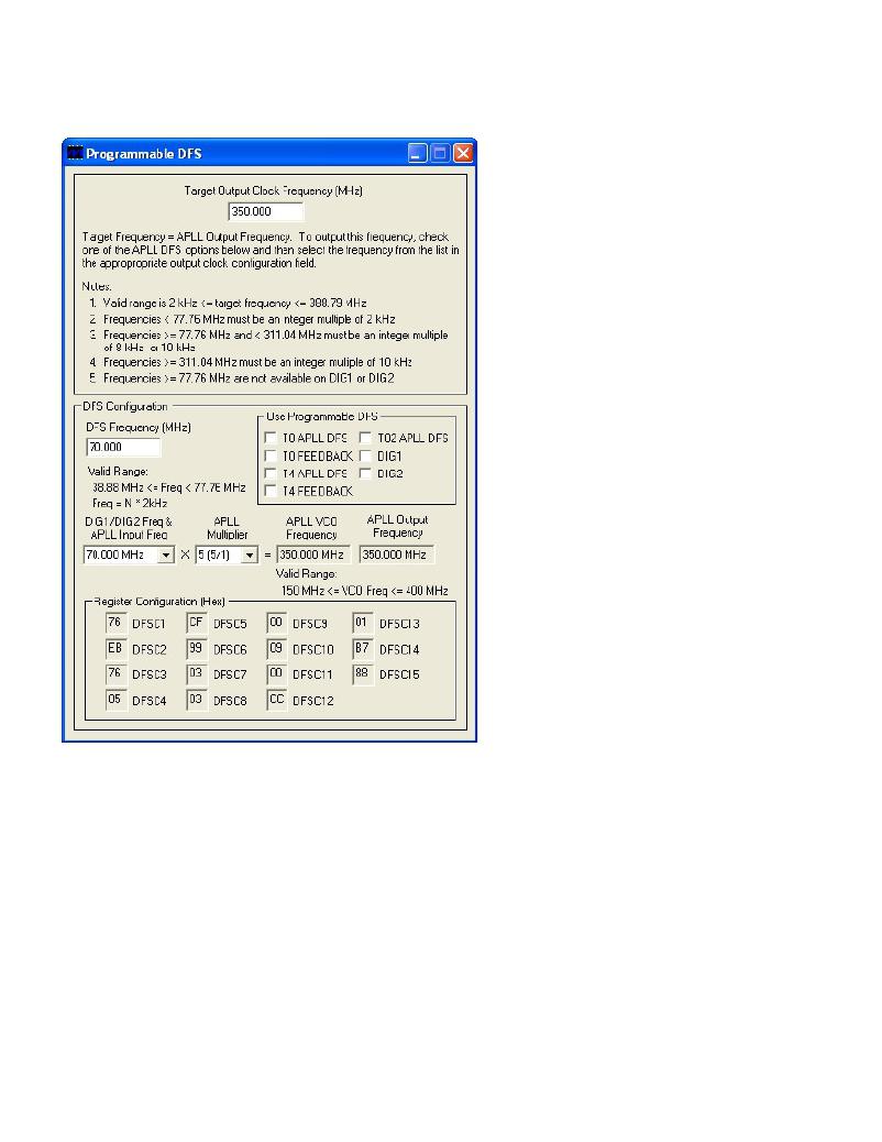
�Whenever� the� T0� APLL� DFS� or� the� T0� APLL2� DFS� are� configured� for� programmable� DFS� operation� (see� Section�
�4.9� ),� their� respective� Input� Freq� and� Output� Freq� fields� specify� their� frequencies� with� a� “P”� prefix� to� indicate� that�
�programmable� DFS� mode� is� enabled.�
�Table� 4-3.� Mapping� Between� T0� APLL� Software� Fields� and� DS3106� Register� Fields�
�SOFTWARE� FIELD�
�Input� Freq�
�Output� Freq�
�DS3106� REGISTER� FIELDS�
�T0CR1:T0FREQ�
�Derived� by� software� from� Input� Freq�
�4.5�
�T4� APLL�
�The� Input� Freq� field� in� the� T4� APLL� box� configures� the� frequency� of� the� T4� APLL� DFS� (refer� to� the� DS3106� data�
�sheet� for� details).� The� APLL� output� frequency� is� always� four� times� the� input� frequency.� When� the� Input� Freq� field�
�is� changed,� the� Output� Freq� field� changes� to� match,� and� all� the� T4� options� in� the� OC3� and� OC6� output� clock�
�combo� boxes� also� change� to� frequencies� derived� from� the� new� T4� APLL� frequency.� These� changes� match� what�
�happens� in� the� DS3106.�
�Whenever� the� T4� APLL� DFS� is� configured� for� programmable� DFS� operation� (see� Section� 4.9� ),� the� Input� Freq� and�
�Output� Freq� fields� specify� their� frequencies� with� a� “P”� prefix� to� indicate� that� programmable� DFS� mode� is� enabled�
�for� the� T4� APLL� DFS.�
�Table� 4-4.� Mapping� Between� T4� APLL� Software� Fields� and� DS3106� Register� Fields�
�SOFTWARE� FIELD�
�Input� Freq�
�Output� Freq�
�DS3106� REGISTER� FIELDS�
�T0CR1:T0FT4�
�Derived� by� software� from� Input� Freq�
�4.6�
�Output� Clocks�
�The� fields� in� the� OUTPUT� CLOCKS� box� configure� the� DS3106’s� output� clocks.� The� DIG1� and� DIG2� fields�
�configure� the� Digital1� and� Digital2� frequency� options� for� OC3� and� OC6� (refer� to� the� DS3106� data� sheet� for� details).�
�The� OC3� and� OC6� fields� specify� the� output� frequencies� for� outputs� OC3� and� OC6.� Note� that� when� the� T0� APLL�
�setting� is� changed,� the� frequencies� of� all� the� T0� options� in� the� OC3� and� OC6� fields� automatically� change� to�
�frequencies� derived� from� the� new� T0� APLL� frequency.� Similarly,� when� the� T4� APLL� setting� is� changed,� the�
�frequencies� of� all� the� T4� options� in� the� OC3� and� OC6� fields� automatically� change� to� frequencies� derived� from� the�
�new� T4� APLL� frequency.� These� changes� match� what� happens� in� the� DS3106.�
�Whenever� the� T0� APLL� DFS,� T4� APLL� DFS,� or� T0� APLL2� DFS� are� configured� for� programmable� DFS� operation�
�(see� Section� 4.9� ),� the� T0,� T4,� and� T02� options,� respectively,� in� the� OC3� and� OC6� fields� change� to� frequencies�
�derived� from� the� programmable� DFS� settings.� These� options� all� have� a� “P”� prefix,� for� example,� “PT0”� or� “PT4”� to�
�indicate� that� they� are� controlled� by� the� programmable� DFS� mode.� Similarly,� whenever� the� DIG1� DFS� or� the� DIG2�
�Rev:� 012208�
�10� of� 32�
�相关PDF资料 |
PDF描述 |
|---|---|
| DS3144DK | KIT DEMO FOR DS3144 |
| DS3150DK | KIT DEMO DS3150 DS3/E3/STS-2 LIU |
| DS3153DK | KIT DEMO FOR DS3153 |
| DS3154DK | KIT DEMO FOR DS3154 |
| DS3170DK | KIT DESIGN FOR DS3170 |
相关代理商/技术参数 |
参数描述 |
|---|---|
| DS3106E12S-3S(621) | 制造商:Amphenol Corporation 功能描述: |
| DS3106F-10SL-3S | 制造商:Amphenol Corporation 功能描述: |
| DS3106F-10SL-4P | 制造商:Amphenol Corporation 功能描述: |
| DS3106F-10SL-4S | 制造商:Amphenol 功能描述:10SL-4 vO Solder 500VDC / 700VAC 13A 125 Silver 制造商:Amphenol 功能描述:10SL-4 vO Solder 500VDC / 700VAC 13A 125 Silver Bulk |
| DS3106F-10SL-4S(621) | 制造商:Amphenol Corporation 功能描述: |
发布紧急采购,3分钟左右您将得到回复。