参数资料
| 型号: | DS3172N+ |
| 厂商: | Maxim Integrated Products |
| 文件页数: | 193/234页 |
| 文件大小: | 0K |
| 描述: | IC TXRX DS3/E3 DUAL 400-BGA |
| 产品培训模块: | Lead (SnPb) Finish for COTS Obsolescence Mitigation Program |
| 标准包装: | 4 |
| 功能: | 单芯片收发器 |
| 接口: | DS3,E3 |
| 电路数: | 2 |
| 电源电压: | 3.135 V ~ 3.465 V |
| 电流 - 电源: | 328mA |
| 工作温度: | -40°C ~ 85°C |
| 安装类型: | 表面贴装 |
| 封装/外壳: | 400-BBGA |
| 供应商设备封装: | 400-PBGA(27x27) |
| 包装: | 管件 |
| 包括: | DS3 调帧器,E3 调帧器,HDLC 控制器,芯片内 BERT |
第1页第2页第3页第4页第5页第6页第7页第8页第9页第10页第11页第12页第13页第14页第15页第16页第17页第18页第19页第20页第21页第22页第23页第24页第25页第26页第27页第28页第29页第30页第31页第32页第33页第34页第35页第36页第37页第38页第39页第40页第41页第42页第43页第44页第45页第46页第47页第48页第49页第50页第51页第52页第53页第54页第55页第56页第57页第58页第59页第60页第61页第62页第63页第64页第65页第66页第67页第68页第69页第70页第71页第72页第73页第74页第75页第76页第77页第78页第79页第80页第81页第82页第83页第84页第85页第86页第87页第88页第89页第90页第91页第92页第93页第94页第95页第96页第97页第98页第99页第100页第101页第102页第103页第104页第105页第106页第107页第108页第109页第110页第111页第112页第113页第114页第115页第116页第117页第118页第119页第120页第121页第122页第123页第124页第125页第126页第127页第128页第129页第130页第131页第132页第133页第134页第135页第136页第137页第138页第139页第140页第141页第142页第143页第144页第145页第146页第147页第148页第149页第150页第151页第152页第153页第154页第155页第156页第157页第158页第159页第160页第161页第162页第163页第164页第165页第166页第167页第168页第169页第170页第171页第172页第173页第174页第175页第176页第177页第178页第179页第180页第181页第182页第183页第184页第185页第186页第187页第188页第189页第190页第191页第192页当前第193页第194页第195页第196页第197页第198页第199页第200页第201页第202页第203页第204页第205页第206页第207页第208页第209页第210页第211页第212页第213页第214页第215页第216页第217页第218页第219页第220页第221页第222页第223页第224页第225页第226页第227页第228页第229页第230页第231页第232页第233页第234页
DS3171/DS3172/DS3173/DS3174
61
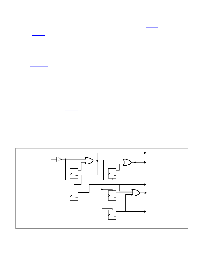
The external
RST pin and the global reset bit in the global configuration register (GL.CR1.RST) are combined to
create an internal global reset signal. The global reset signal resets all the status and control registers on the chip,
except the GL.CR1.RST bit, to their default values and resets all the other flops in the global logic and ports to their
reset values. The processor bus output signals are also forced to be HIZ when the
RST pin is active (low). The
global reset bit (GL.CR1.RST) stays set after a one is written to it, but is reset to zero when the external
RST pin is
active or when a zero is written to it.
At the port level, the global reset signal combines with the port-reset bit in the port control register
(PORT.CR1.RST) to create a port-reset signal. The port reset signal resets all the status and control registers on
the port to their default values and resets all the other flops, except PORT.CR1.RST, to their reset values. The port
reset bit (PORT.CR1.RST) stays set after a one is written to it, but is reset to zero when the global reset signal is
active or when a zero is written to it.
The data path reset function is a little different from the “general” reset function. The data path reset signal does not
reset the control register bits, but it does reset all of the status registers, counters and flops, the “general” reset
signal resets everything including the control register bits, excluding the reset bit. All clocks are functional, being
controlled by configuration bits, while data path reset is active. The LIU and CLAD circuits will be operating
normally during data path reset, which allows the internal phase locked loops to settle as quickly as possible. The
LIU will be sending all zeros (LOS) since data path reset will be forcing the transmit TPOSn and TNEGn to logic
zero. (NOTE: The BERT data path and control registers are reset when the global data path reset or the port data
path reset or the port power-down signal is active.)
The global data path reset bit (GL.CR1.RSTDP) gets set to one when the global reset signal is active. The port
data path reset bit (PORT.CR1.RSTDP) and the port power-down bit (PORT.CR1.PD) bit get set to one when the
global reset signal is active or the port reset signal is active. These control bits will be cleared when a zero is
written to them if the global reset signal or the port-reset signal is not active. The global data path reset signal is
active when the global data path reset bit is set. The port data path reset signal is active when either the global
data path reset bit or the port data path reset bit is set. The port power-down signal is active when the port power-
down bit is set.
Figure 10-5. Reset Sources
Q
SET
CLR
D
Q
SET
CLR
D
Q
SET
CLR
D
Q
SET
CLR
D
RST pin
Global Reset
Port Reset
Global Data Path Reset
Port Data Path Reset
GL.CR1
. RST
GL.CR1
. RSTDP
PORT.CR1
.
RST
PORT.CR1
.
RSTDP
NOTE: Assumes
active high signals
Q
SET
CLR
D
Port Power Down
PORT.CR1
. PD
相关PDF资料 |
PDF描述 |
|---|---|
| DS3181N+ | IC ATM/PACKET PHY W/LIU 400PBGA |
| DS32512N+ | IC LIU DS3/E3/STS-1 12P 484-BGA |
| DS3254N+ | IC LIU DS3/E3/STS-1 144-CSBGA |
| DS33M33N+ | IC MAPPER ETHERNET 256CSBGA |
| DS33R11+CJ2 | IC ETH TXRX T1/E1/J1 256-BGA |
相关代理商/技术参数 |
参数描述 |
|---|---|
| DS3172N+ | 功能描述:网络控制器与处理器 IC Dual DS3/E3 Single Chip Transceiver RoHS:否 制造商:Micrel 产品:Controller Area Network (CAN) 收发器数量: 数据速率: 电源电流(最大值):595 mA 最大工作温度:+ 85 C 安装风格:SMD/SMT 封装 / 箱体:PBGA-400 封装:Tray |
| DS3173 | 功能描述:网络控制器与处理器 IC Triple DS3/E3 Single Chip Transceiver RoHS:否 制造商:Micrel 产品:Controller Area Network (CAN) 收发器数量: 数据速率: 电源电流(最大值):595 mA 最大工作温度:+ 85 C 安装风格:SMD/SMT 封装 / 箱体:PBGA-400 封装:Tray |
| DS3173N | 功能描述:网络控制器与处理器 IC Triple DS3/E3 Single Chip Transceiver RoHS:否 制造商:Micrel 产品:Controller Area Network (CAN) 收发器数量: 数据速率: 电源电流(最大值):595 mA 最大工作温度:+ 85 C 安装风格:SMD/SMT 封装 / 箱体:PBGA-400 封装:Tray |
| DS3174 | 功能描述:网络控制器与处理器 IC Quad DS3/E3 Single Chip Transceiver RoHS:否 制造商:Micrel 产品:Controller Area Network (CAN) 收发器数量: 数据速率: 电源电流(最大值):595 mA 最大工作温度:+ 85 C 安装风格:SMD/SMT 封装 / 箱体:PBGA-400 封装:Tray |
| DS3174+ | 功能描述:网络控制器与处理器 IC Quad DS3/E3 Single Chip Transceiver RoHS:否 制造商:Micrel 产品:Controller Area Network (CAN) 收发器数量: 数据速率: 电源电流(最大值):595 mA 最大工作温度:+ 85 C 安装风格:SMD/SMT 封装 / 箱体:PBGA-400 封装:Tray |
发布紧急采购,3分钟左右您将得到回复。