- 您现在的位置:买卖IC网 > Datasheet目录323 > DSP56311EVM (Freescale Semiconductor)KIT EVALUATION FOR DSP56311 Datasheet资料下载
参数资料
| 型号: | DSP56311EVM |
| 厂商: | Freescale Semiconductor |
| 文件页数: | 97/360页 |
| 文件大小: | 0K |
| 描述: | KIT EVALUATION FOR DSP56311 |
| 标准包装: | 1 |
| 类型: | DSP |
| 适用于相关产品: | DSP56311 |
| 所含物品: | 模块板、安装指南、电源、缆线、软件等 |
第1页第2页第3页第4页第5页第6页第7页第8页第9页第10页第11页第12页第13页第14页第15页第16页第17页第18页第19页第20页第21页第22页第23页第24页第25页第26页第27页第28页第29页第30页第31页第32页第33页第34页第35页第36页第37页第38页第39页第40页第41页第42页第43页第44页第45页第46页第47页第48页第49页第50页第51页第52页第53页第54页第55页第56页第57页第58页第59页第60页第61页第62页第63页第64页第65页第66页第67页第68页第69页第70页第71页第72页第73页第74页第75页第76页第77页第78页第79页第80页第81页第82页第83页第84页第85页第86页第87页第88页第89页第90页第91页第92页第93页第94页第95页第96页当前第97页第98页第99页第100页第101页第102页第103页第104页第105页第106页第107页第108页第109页第110页第111页第112页第113页第114页第115页第116页第117页第118页第119页第120页第121页第122页第123页第124页第125页第126页第127页第128页第129页第130页第131页第132页第133页第134页第135页第136页第137页第138页第139页第140页第141页第142页第143页第144页第145页第146页第147页第148页第149页第150页第151页第152页第153页第154页第155页第156页第157页第158页第159页第160页第161页第162页第163页第164页第165页第166页第167页第168页第169页第170页第171页第172页第173页第174页第175页第176页第177页第178页第179页第180页第181页第182页第183页第184页第185页第186页第187页第188页第189页第190页第191页第192页第193页第194页第195页第196页第197页第198页第199页第200页第201页第202页第203页第204页第205页第206页第207页第208页第209页第210页第211页第212页第213页第214页第215页第216页第217页第218页第219页第220页第221页第222页第223页第224页第225页第226页第227页第228页第229页第230页第231页第232页第233页第234页第235页第236页第237页第238页第239页第240页第241页第242页第243页第244页第245页第246页第247页第248页第249页第250页第251页第252页第253页第254页第255页第256页第257页第258页第259页第260页第261页第262页第263页第264页第265页第266页第267页第268页第269页第270页第271页第272页第273页第274页第275页第276页第277页第278页第279页第280页第281页第282页第283页第284页第285页第286页第287页第288页第289页第290页第291页第292页第293页第294页第295页第296页第297页第298页第299页第300页第301页第302页第303页第304页第305页第306页第307页第308页第309页第310页第311页第312页第313页第314页第315页第316页第317页第318页第319页第320页第321页第322页第323页第324页第325页第326页第327页第328页第329页第330页第331页第332页第333页第334页第335页第336页第337页第338页第339页第340页第341页第342页第343页第344页第345页第346页第347页第348页第349页第350页第351页第352页第353页第354页第355页第356页第357页第358页第359页第360页
��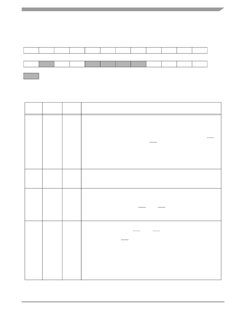 �
�
�Bus� Interface� Unit� (BIU)� Registers�
�Note:�
�To� prevent� improper� device� operation,� you� must� guarantee� that� all� the� DCR� bits� except�
�BSTR� are� not� changed� during� a� DRAM� access.�
�23�
�BRP�
�11�
�22�
�BRF7�
�10�
�21�
�BRF6�
�9�
�20�
�BRF5�
�8�
�19�
�BRF4�
�7�
�18�
�BRF3�
�6�
�17�
�BRF2�
�5�
�16�
�BRF1�
�4�
�15�
�BRF0�
�3�
�14�
�BSTR�
�2�
�13�
�BREN�
�1�
�12�
�BME�
�0�
�BPLE�
�BPS1�
�BPS0�
�BRW1�
�BRW0�
�BCW1�
�BCW0�
�Reserved� bit.� Read� as� zero;� write� to� zero� for� future� compatibility�
�Figure� 4-7.� DRAM� Control� Register� (DCR)�
�Table� 4-9.� DRAM� Control� Register� (DCR)� Bit� Definitions�
�Bit�
�Number�
�23�
�Bit� Name�
�BRP�
�Reset�
�Value�
�0�
�Bus� Refresh� Prescaler�
�Description�
�Controls� a� prescaler� in� series� with� the� refresh� clock� divider.� If� BPR� is� set,� a�
�divide-by-64� prescaler� is� connected� in� series� with� the� refresh� clock� divider.� If� BPR� is�
�cleared,� the� prescaler� is� bypassed.� The� refresh� request� rate� (in� clock� cycles)� is� the�
�value� written� to� BRF[7–0]� bits� +� 1,� multiplied� by� 64� (if� BRP� is� set)� or� by� one� (if� BRP� is�
�cleared).� When� programming� the� periodic� refresh� rate,� you� must� consider� the� RAS�
�time-out� period.� Hardware� support� for� the� RAS� time-out� restriction� does� not� exist� .�
�Note:�
�Refresh� requests� are� not� accumulated� and,� therefore,� in� a� fast� refresh� request�
�rate� not� all� the� refresh� requests� are� served� (for� example,� the� combination�
�BRF[7–0]� =� $00� and� BRP� =� 0� generates� a� refresh� request� every� clock� cycle,�
�but� a� refresh� access� takes� at� least� five� clock� cycles).�
�22–15�
�BRF[7–0]�
�0�
�Bus� Refresh� Rate�
�Controls� the� refresh� request� rate.� The� BRF[7–0]� bits� specify� a� divide� rate� of� 1–256�
�(BRF[7–0]� =� $00–$FF).� A� refresh� request� is� generated� each� time� the� refresh� counter�
�reaches� zero� if� the� refresh� counter� is� enabled� (BRE� =� 1).�
�14�
�BSTR�
�0�
�Bus� Software� Triggered� Reset�
�Generates� a� software-triggered� refresh� request.� When� BSTR� is� set,� a� refresh� request�
�is� generated� and� a� refresh� access� is� executed� to� all� DRAM� banks� (the� exact� timing� of�
�the� refresh� access� depends� on� the� pending� external� accesses� and� the� status� of� the�
�BME� bit).� After� the� refresh� access� (CAS� before� RAS)� is� executed,� the� DRAM� controller�
�hardware� clears� the� BSTR� bit.� The� refresh� cycle� length� depends� on� the� BRW[1–0]� bits�
�(a� refresh� access� is� as� long� as� the� out-of-page� access).�
�13�
�BREN�
�0�
�Bus� Refresh� Enable�
�Enables/disables� the� internal� refresh� counter.� When� BREN� is� set,� the� refresh� counter� is�
�enabled� and� a� refresh� request� (CAS� before� RAS)� is� generated� each� time� the� refresh�
�counter� reaches� zero.� A� refresh� cycle� occurs� for� all� DRAM� banks� together� (that� is,� all�
�pins� that� are� defined� as� RAS� are� asserted� together).� When� this� bit� is� cleared,� the�
�refresh� counter� is� disabled� and� a� refresh� request� may� be� software� triggered� by� using�
�the� BSTR� bit.� In� a� system� in� which� DSPs� share� the� same� DRAM,� the� DRAM� controller�
�of� more� than� one� DSP� may� be� active,� but� it� is� recommended� that� only� one� DSP� have�
�its� BREN� bit� set� and� that� bus� mastership� is� requested� for� a� refresh� access.� If� BREN� is�
�set� and� a� WAIT� instruction� is� executed,� periodic� refresh� is� still� generated� each� time� the�
�refresh� counter� reaches� zero.� If� BREN� is� set� and� a� STOP� instruction� is� executed,�
�periodic� refresh� is� not� generated� and� the� refresh� counter� is� disabled.� The� contents� of�
�the� DRAM� are� lost.�
�DSP56311� User’s� Manual,� Rev.� 2�
�Freescale� Semiconductor�
�4-23�
�相关PDF资料 |
PDF描述 |
|---|---|
| DSPAUDIOEVMMB1E | BOARD MOTHER DSP563XX |
| DSPIC30F2010 DEVELOPMENT KIT | KIT DEV EMBEDDED C |
| DSTRM-KT-0181A | DSTREAM DEBUG AND TRACE UNIT |
| DSUT1CSU | SURGE SUPPR NETWORK W/GROUND |
| DTEL2 | SURGE SUPPRESSOR PHONE RJ11/RJ45 |
相关代理商/技术参数 |
参数描述 |
|---|---|
| DSP56311EVMIG_D | 制造商:未知厂家 制造商全称:未知厂家 功能描述:DSP56311EVMIG DSP56311EVM Sample Code |
| DSP56311EVMUM | 制造商:未知厂家 制造商全称:未知厂家 功能描述:DSP56311 Evaluation Module Hardware Reference Manual |
| DSP56311FACT | 制造商:未知厂家 制造商全称:未知厂家 功能描述:DSP56311 Higher performance programmable DSP for demanding voice and data applications |
| DSP56311UM | 制造商:未知厂家 制造商全称:未知厂家 功能描述:DSP56311 24-Bit Digital Signal Processor Users Manual |
| DSP56311UMAD | 制造商:未知厂家 制造商全称:未知厂家 功能描述:DSP56311 Users Manual Addendum |
发布紧急采购,3分钟左右您将得到回复。