- 您现在的位置:买卖IC网 > PDF目录11649 > DSP56F826BU80E (Freescale Semiconductor)IC DSP 80MHZ 64KB FLASH 100LQFP PDF资料下载
参数资料
| 型号: | DSP56F826BU80E |
| 厂商: | Freescale Semiconductor |
| 文件页数: | 8/56页 |
| 文件大小: | 0K |
| 描述: | IC DSP 80MHZ 64KB FLASH 100LQFP |
| 标准包装: | 90 |
| 系列: | 56F8xx |
| 核心处理器: | 56800 |
| 芯体尺寸: | 16-位 |
| 速度: | 80MHz |
| 连通性: | EBI/EMI,SCI,SPI,SSI |
| 外围设备: | POR,WDT |
| 输入/输出数: | 46 |
| 程序存储器容量: | 67KB(33.5K x 16) |
| 程序存储器类型: | 闪存 |
| RAM 容量: | 4.5K x 16 |
| 电压 - 电源 (Vcc/Vdd): | 2.25 V ~ 2.75 V |
| 振荡器型: | 外部 |
| 工作温度: | -40°C ~ 85°C |
| 封装/外壳: | 100-LQFP |
| 包装: | 托盘 |
第1页第2页第3页第4页第5页第6页第7页当前第8页第9页第10页第11页第12页第13页第14页第15页第16页第17页第18页第19页第20页第21页第22页第23页第24页第25页第26页第27页第28页第29页第30页第31页第32页第33页第34页第35页第36页第37页第38页第39页第40页第41页第42页第43页第44页第45页第46页第47页第48页第49页第50页第51页第52页第53页第54页第55页第56页
56F826 Technical Data, Rev. 14
16
Freescale Semiconductor
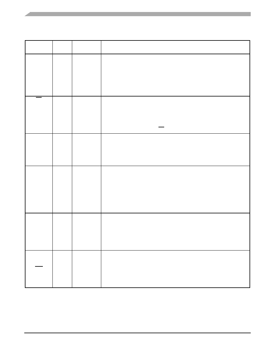
MISO
(GPIOF6)
86
Input/Output
SPI Master In/Slave Out (MISO)—This serial data pin is an input to a master
device and an output from a slave device. The MISO line of a slave device is
placed in the high-impedance state if the slave device is not selected.
Port F GPIO—This General Purpose I/O (GPIO) pin can be individually
programmed as input or output.
After reset, the default state is MISO.
SS
(GPIOF7)
87
Input
Input/Output
SPI Slave Select—In master mode, this pin is used to arbitrate multiple masters.
In slave mode, this pin is used to select the slave.
Port F GPIO—This General Purpose I/O (GPIO) pin can be individually
programmed as input or output.
After reset, the default state is SS.
TXD0
(SCLK0)
97
Output
Input/Output
Transmit Data (TXD0)—transmit data output
SPI Serial Clock—In master mode, this pin serves as an output, clocking slaved
listeners. In slave mode, this pin serves as the data clock input.
After reset, the default state is SCI output.
RXD0
(MOSI0)
96
Input
Input/Output
Receive Data (RXD0)— receive data input
SPI Master Out/Slave In—This serial data pin is an output from a master
device, and an input to a slave device. The master device places data on the
MOSI line one half-cycle before the clock edge the slave device uses to latch the
data.
After reset, the default state is SCI input.
TXD1
(MISO0)
93
Output
Input/Output
Transmit Data (TXD1)—transmit data output
SPI Master In/Slave Out—This serial data pin is an input to a master device and
an output from a slave device. The MISO line of a slave device is placed in the
high-impedance state if the slave device is not selected.
After reset, the default state is SCI output.
RXD1
(SS0)
92
Input
(Schmitt)
Input
Receive Data (RXD1)— receive data input
SPI Slave Select—In master mode, this pin is used to arbitrate multiple masters.
In slave mode, this pin is used to select the slave.
After reset, the default state is SCI input.
Table 2-1 56F826 Signal and Package Information for the 100 Pin LQFP (Continued)
Signal
Name
Pin No.
Type
Description
相关PDF资料 |
PDF描述 |
|---|---|
| MC908AS60ACFNE | IC MCU 60K FLASH 8.4MHZ 52PLCC |
| MC9S12XDT256MAA | IC MCU 256K FLASH 80-QFP |
| MC9S12XD256MAG | IC MCU 256K FLASH 144-LQFP |
| MC9S12XDT512CAA | IC MCU 512K FLASH 80-QFP |
| MC56F8347VPYE | IC DSP 16BIT 60MHZ 160-LQFP |
相关代理商/技术参数 |
参数描述 |
|---|---|
| DSP56F826BU80E | 制造商:Freescale Semiconductor 功能描述:Digital Signal Processor IC DSP Type:Cor |
| DSP56F826BU80E | 制造商:Freescale Semiconductor 功能描述:DSP LQFP100 3.6V |
| DSP56F826D | 制造商:MOTOROLA 制造商全称:Motorola, Inc 功能描述:Preliminary Technical Data DSP56F826 16-bit Digital Signal Processor |
| DSP56F826E | 制造商:FREESCALE 制造商全称:Freescale Semiconductor, Inc 功能描述:16-bit Digital Signal Controllers |
| DSP56F826EVM | 功能描述:开发板和工具包 - 其他处理器 Evaluation Kit For DSP56F826 RoHS:否 制造商:Freescale Semiconductor 产品:Development Systems 工具用于评估:P3041 核心:e500mc 接口类型:I2C, SPI, USB 工作电源电压: |
发布紧急采购,3分钟左右您将得到回复。