- 您现在的位置:买卖IC网 > PDF目录295885 > EP1SGX25DF1020C6ES (ALTERA CORP) FPGA, PBGA1020 PDF资料下载
参数资料
| 型号: | EP1SGX25DF1020C6ES |
| 厂商: | ALTERA CORP |
| 元件分类: | FPGA |
| 英文描述: | FPGA, PBGA1020 |
| 封装: | 33 X 33 MM, 1 MM PITCH, FBGA-1020 |
| 文件页数: | 120/279页 |
| 文件大小: | 3671K |
| 代理商: | EP1SGX25DF1020C6ES |
第1页第2页第3页第4页第5页第6页第7页第8页第9页第10页第11页第12页第13页第14页第15页第16页第17页第18页第19页第20页第21页第22页第23页第24页第25页第26页第27页第28页第29页第30页第31页第32页第33页第34页第35页第36页第37页第38页第39页第40页第41页第42页第43页第44页第45页第46页第47页第48页第49页第50页第51页第52页第53页第54页第55页第56页第57页第58页第59页第60页第61页第62页第63页第64页第65页第66页第67页第68页第69页第70页第71页第72页第73页第74页第75页第76页第77页第78页第79页第80页第81页第82页第83页第84页第85页第86页第87页第88页第89页第90页第91页第92页第93页第94页第95页第96页第97页第98页第99页第100页第101页第102页第103页第104页第105页第106页第107页第108页第109页第110页第111页第112页第113页第114页第115页第116页第117页第118页第119页当前第120页第121页第122页第123页第124页第125页第126页第127页第128页第129页第130页第131页第132页第133页第134页第135页第136页第137页第138页第139页第140页第141页第142页第143页第144页第145页第146页第147页第148页第149页第150页第151页第152页第153页第154页第155页第156页第157页第158页第159页第160页第161页第162页第163页第164页第165页第166页第167页第168页第169页第170页第171页第172页第173页第174页第175页第176页第177页第178页第179页第180页第181页第182页第183页第184页第185页第186页第187页第188页第189页第190页第191页第192页第193页第194页第195页第196页第197页第198页第199页第200页第201页第202页第203页第204页第205页第206页第207页第208页第209页第210页第211页第212页第213页第214页第215页第216页第217页第218页第219页第220页第221页第222页第223页第224页第225页第226页第227页第228页第229页第230页第231页第232页第233页第234页第235页第236页第237页第238页第239页第240页第241页第242页第243页第244页第245页第246页第247页第248页第249页第250页第251页第252页第253页第254页第255页第256页第257页第258页第259页第260页第261页第262页第263页第264页第265页第266页第267页第268页第269页第270页第271页第272页第273页第274页第275页第276页第277页第278页第279页
6–4
Altera Corporation
Stratix GX Device Handbook, Volume 1
August 2005
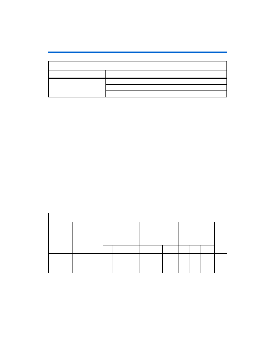
Operating Conditions
Refclkb
Dedicated transceiver
clock termination
Commercial and industrial, 100-
Ω setting
103
108
113
Ω
Commercial and industrial, 120-
Ω setting
120
128
134
Ω
Commercial and industrial, 150-
Ω setting
149
158
167
Ω
Notes to Tables 6–1 through 6–6:
(1)
(2)
Conditions beyond those listed in Table 6–1 may cause permanent damage to a device. Additionally, device
operation at the absolute maximum ratings for extended periods of time may have adverse affects on the device.
(3)
Minimum DC input is –0.5 V. During transitions, the inputs may undershoot to –0.5 V or overshoot to 4.6 V for
input currents less than 100 mA and periods shorter than 20 ns. (The information in this note does not include the
transceiver pins. See note 13 for information about the transient voltage on the transceiver pins.)
(4)
Maximum VCC rise time is 100 ms, and VCC must rise monotonically.
(5)
VCCIO maximum and minimum conditions for LVPECL, LVDS, and 3.3-V PCML are shown in parentheses.
(6)
All pins, including dedicated inputs, clock, I/O, and JTAG pins, may be driven before VCCINT and VCCIO are
powered.
(7)
Typical values are for TA = 25° C, VCCINT = 1.5 V, and VCCIO = 1.5 V, 1.8 V, 2.5 V, and 3.3 V.
(8)
This value is specified for normal device operation. The value may vary during power-up. This applies for all VCCIO
settings (3.3, 2.5, 1.8, and 1.5 V).
(9)
Pin pull-up resistance values decrease if an external source drives the pin higher than VCCIO.
(10) The device can tolerate prolonged operation at this absolute maximum, as long as the maximum specification is
not violated.
(11) Each useable quad requires its own RREF resistor path to ground. For example, the “D” in the EP1SGX25DC1020
device code means it has two useable quad so two different RREF pins must be connected to a RREF resistor each to
ground. The DC signal on the RREF pin must be as clean as possible. Ensure that no noise is coupled to this pin.
(12) The Stratix GX device’s recommended operating conditions do not include the transceiver. Refer to Tables 6–4 to
(13) Minimum DC input to the transceiver pins is –0.5 V. During transitions, the transceiver pins may undershoot to
–0.5 V or overshoot to 3.5 V for input currents less than 100 mA and periods shorter than 20 ns.
Table 6–7. Stratix GX Transceiver Block AC Specification (Part 1 of 7)
Symbol /
Description
Conditions
-5 Commercial
Speed Grade (1)
-6 Commercial &
Industrial Speed
Grade
-7 Commercial &
Industrial Speed
Grade
Unit
Min
Typ
Max
Min
Typ
Max
Min
Typ
Max
Power per
quadrant
(PCS +
PMA)
3.125 Gbps, 400-
mV Vod
0 pre-emphasis
450
mW
Table 6–6. Stratix GX Transceiver Block On-Chip Termination (Part 2 of 2)
Symbol
Parameter
Conditions
Min
Typ
Max
Units
相关PDF资料 |
PDF描述 |
|---|---|
| EP1SGX25DF1020C7ES | FPGA, PBGA1020 |
| EP1SGX25DF1020I5ES | FPGA, PBGA1020 |
| EP1SGX25DF1020I5N | FPGA, PBGA1020 |
| EP1SGX25DF1020I6ES | FPGA, PBGA1020 |
| EP1SGX25DF1020I6N | FPGA, PBGA1020 |
相关代理商/技术参数 |
参数描述 |
|---|---|
| EP1SGX25DF1020C6N | 功能描述:FPGA - 现场可编程门阵列 FPGA - Stratix I GX 2566 LABs 607 IOs RoHS:否 制造商:Altera Corporation 系列:Cyclone V E 栅极数量: 逻辑块数量:943 内嵌式块RAM - EBR:1956 kbit 输入/输出端数量:128 最大工作频率:800 MHz 工作电源电压:1.1 V 最大工作温度:+ 70 C 安装风格:SMD/SMT 封装 / 箱体:FBGA-256 |
| EP1SGX25DF1020C7 | 功能描述:FPGA - 现场可编程门阵列 FPGA - Stratix I GX 2566 LABs 607 IOs RoHS:否 制造商:Altera Corporation 系列:Cyclone V E 栅极数量: 逻辑块数量:943 内嵌式块RAM - EBR:1956 kbit 输入/输出端数量:128 最大工作频率:800 MHz 工作电源电压:1.1 V 最大工作温度:+ 70 C 安装风格:SMD/SMT 封装 / 箱体:FBGA-256 |
| EP1SGX25DF1020C7N | 功能描述:FPGA - 现场可编程门阵列 FPGA - Stratix I GX 2566 LABs 607 IOs RoHS:否 制造商:Altera Corporation 系列:Cyclone V E 栅极数量: 逻辑块数量:943 内嵌式块RAM - EBR:1956 kbit 输入/输出端数量:128 最大工作频率:800 MHz 工作电源电压:1.1 V 最大工作温度:+ 70 C 安装风格:SMD/SMT 封装 / 箱体:FBGA-256 |
| EP1SGX25DF672C5 | 功能描述:FPGA - 现场可编程门阵列 FPGA - Stratix I GX 2566 LABs 455 IOs RoHS:否 制造商:Altera Corporation 系列:Cyclone V E 栅极数量: 逻辑块数量:943 内嵌式块RAM - EBR:1956 kbit 输入/输出端数量:128 最大工作频率:800 MHz 工作电源电压:1.1 V 最大工作温度:+ 70 C 安装风格:SMD/SMT 封装 / 箱体:FBGA-256 |
| EP1SGX25DF672C5N | 功能描述:FPGA - 现场可编程门阵列 FPGA - Stratix I GX 2566 LABs 455 IOs RoHS:否 制造商:Altera Corporation 系列:Cyclone V E 栅极数量: 逻辑块数量:943 内嵌式块RAM - EBR:1956 kbit 输入/输出端数量:128 最大工作频率:800 MHz 工作电源电压:1.1 V 最大工作温度:+ 70 C 安装风格:SMD/SMT 封装 / 箱体:FBGA-256 |
发布紧急采购,3分钟左右您将得到回复。