- 您现在的位置:买卖IC网 > PDF目录295885 > EP1SGX25DF1020C6ES (ALTERA CORP) FPGA, PBGA1020 PDF资料下载
参数资料
| 型号: | EP1SGX25DF1020C6ES |
| 厂商: | ALTERA CORP |
| 元件分类: | FPGA |
| 英文描述: | FPGA, PBGA1020 |
| 封装: | 33 X 33 MM, 1 MM PITCH, FBGA-1020 |
| 文件页数: | 93/279页 |
| 文件大小: | 3671K |
| 代理商: | EP1SGX25DF1020C6ES |
第1页第2页第3页第4页第5页第6页第7页第8页第9页第10页第11页第12页第13页第14页第15页第16页第17页第18页第19页第20页第21页第22页第23页第24页第25页第26页第27页第28页第29页第30页第31页第32页第33页第34页第35页第36页第37页第38页第39页第40页第41页第42页第43页第44页第45页第46页第47页第48页第49页第50页第51页第52页第53页第54页第55页第56页第57页第58页第59页第60页第61页第62页第63页第64页第65页第66页第67页第68页第69页第70页第71页第72页第73页第74页第75页第76页第77页第78页第79页第80页第81页第82页第83页第84页第85页第86页第87页第88页第89页第90页第91页第92页当前第93页第94页第95页第96页第97页第98页第99页第100页第101页第102页第103页第104页第105页第106页第107页第108页第109页第110页第111页第112页第113页第114页第115页第116页第117页第118页第119页第120页第121页第122页第123页第124页第125页第126页第127页第128页第129页第130页第131页第132页第133页第134页第135页第136页第137页第138页第139页第140页第141页第142页第143页第144页第145页第146页第147页第148页第149页第150页第151页第152页第153页第154页第155页第156页第157页第158页第159页第160页第161页第162页第163页第164页第165页第166页第167页第168页第169页第170页第171页第172页第173页第174页第175页第176页第177页第178页第179页第180页第181页第182页第183页第184页第185页第186页第187页第188页第189页第190页第191页第192页第193页第194页第195页第196页第197页第198页第199页第200页第201页第202页第203页第204页第205页第206页第207页第208页第209页第210页第211页第212页第213页第214页第215页第216页第217页第218页第219页第220页第221页第222页第223页第224页第225页第226页第227页第228页第229页第230页第231页第232页第233页第234页第235页第236页第237页第238页第239页第240页第241页第242页第243页第244页第245页第246页第247页第248页第249页第250页第251页第252页第253页第254页第255页第256页第257页第258页第259页第260页第261页第262页第263页第264页第265页第266页第267页第268页第269页第270页第271页第272页第273页第274页第275页第276页第277页第278页第279页
4–116
Altera Corporation
Stratix GX Device Handbook, Volume 1
February 2005
I/O Structure
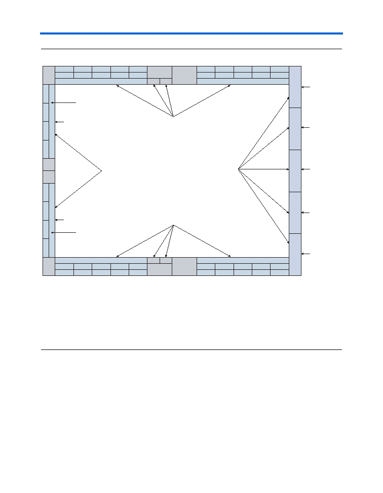
Figure 4–69. Stratix GX I/O Banks
Notes to Figure 4–69:
(1)
Figure 4–69 is a top view of the Stratix GX silicon die.
(2)
Banks 9 through 12 are enhanced PLL external clock output banks.
(3)
If the high-speed differential I/O pins are not used for high-speed differential signaling, they can support all of the
I/O standards except HSTL class I and II, GTL, SSTL-18 Class II, PCI, PCI-X, and AGP 1×/2×.
(4)
For guidelines for placing single-ended I/O pads next to differential I/O pads, see the Selectable I/O Standards in
Stratix & Stratix GX Devices chapter in the Stratix GX Device Handbook, Volume 2.
(5)
These I/O banks in Stratix GX devices also support the LVDS, LVPECL, and 3.3-V PCML I/O standards on reference
clocks and receiver input pins (AC coupled)
LVDS, LVPECL, 3.3-V PCML,
and HyperTransport I/O Block
and Regular I/O Pins (3)
I/O Banks 3, 4, 9 & 10 Support
All Single-Ended I/O Standards (2)
I/O Banks 7, 8, 11 & 12 Support
All Single-Ended I/O Standards (2)
I/O Banks 1 and 2 Support All
Single-Ended I/O Standards Except
Differential HSTL Output Clocks,
Differential SSTL-2 Output Clocks,
HSTL Class II, GTL, SSTL-18 Class II,
PCI, PCI-X, and AGP 1
×/2×
DQST9
DQST8
DQST7
DQST6
DQST5
DQST4
DQST3
DQST2
DQST1
DQST0
PLL5
VREF1B3
VREF2B3
VREF3B3
VREF4B3
VREF5B3
VREF1B4
VREF2B4
VREF3B4
VREF4B4
VREF5B4
VREF5B8
VREF4B8
VREF3B8
VREF2B8
VREF1B8
VREF5B7
VREF4B7
VREF3B7
VREF2B7
VREF1B7
PLL6
DQSB9
DQSB8
DQSB7
DQSB6
DQSB5
DQSB4
DQSB3
DQSB2
DQSB1
DQSB0
910
VREF1B2
VREF2B2
VREF3B2
VREF4B2
VREF1B1
VREF2B1
VREF3B1
VREF4B1
PLL1
PLL2
Bank
1
Bank
2
Bank 3
Bank 4
11
12
Bank 8
Bank 7
LVDS, LVPECL, 3.3-V PCML,
and HyperTransport I/O Block
and Regular I/O Pins (3)
PLL7
PLL8
PLL12
PLL11
(4)
I/O Bank 13 (5)
I/O Bank 14 (5)
I/O Bank 17 (5)
I/O Bank 16 (5)
I/O Bank 15 (5)
1.5-V PCML (5)
相关PDF资料 |
PDF描述 |
|---|---|
| EP1SGX25DF1020C7ES | FPGA, PBGA1020 |
| EP1SGX25DF1020I5ES | FPGA, PBGA1020 |
| EP1SGX25DF1020I5N | FPGA, PBGA1020 |
| EP1SGX25DF1020I6ES | FPGA, PBGA1020 |
| EP1SGX25DF1020I6N | FPGA, PBGA1020 |
相关代理商/技术参数 |
参数描述 |
|---|---|
| EP1SGX25DF1020C6N | 功能描述:FPGA - 现场可编程门阵列 FPGA - Stratix I GX 2566 LABs 607 IOs RoHS:否 制造商:Altera Corporation 系列:Cyclone V E 栅极数量: 逻辑块数量:943 内嵌式块RAM - EBR:1956 kbit 输入/输出端数量:128 最大工作频率:800 MHz 工作电源电压:1.1 V 最大工作温度:+ 70 C 安装风格:SMD/SMT 封装 / 箱体:FBGA-256 |
| EP1SGX25DF1020C7 | 功能描述:FPGA - 现场可编程门阵列 FPGA - Stratix I GX 2566 LABs 607 IOs RoHS:否 制造商:Altera Corporation 系列:Cyclone V E 栅极数量: 逻辑块数量:943 内嵌式块RAM - EBR:1956 kbit 输入/输出端数量:128 最大工作频率:800 MHz 工作电源电压:1.1 V 最大工作温度:+ 70 C 安装风格:SMD/SMT 封装 / 箱体:FBGA-256 |
| EP1SGX25DF1020C7N | 功能描述:FPGA - 现场可编程门阵列 FPGA - Stratix I GX 2566 LABs 607 IOs RoHS:否 制造商:Altera Corporation 系列:Cyclone V E 栅极数量: 逻辑块数量:943 内嵌式块RAM - EBR:1956 kbit 输入/输出端数量:128 最大工作频率:800 MHz 工作电源电压:1.1 V 最大工作温度:+ 70 C 安装风格:SMD/SMT 封装 / 箱体:FBGA-256 |
| EP1SGX25DF672C5 | 功能描述:FPGA - 现场可编程门阵列 FPGA - Stratix I GX 2566 LABs 455 IOs RoHS:否 制造商:Altera Corporation 系列:Cyclone V E 栅极数量: 逻辑块数量:943 内嵌式块RAM - EBR:1956 kbit 输入/输出端数量:128 最大工作频率:800 MHz 工作电源电压:1.1 V 最大工作温度:+ 70 C 安装风格:SMD/SMT 封装 / 箱体:FBGA-256 |
| EP1SGX25DF672C5N | 功能描述:FPGA - 现场可编程门阵列 FPGA - Stratix I GX 2566 LABs 455 IOs RoHS:否 制造商:Altera Corporation 系列:Cyclone V E 栅极数量: 逻辑块数量:943 内嵌式块RAM - EBR:1956 kbit 输入/输出端数量:128 最大工作频率:800 MHz 工作电源电压:1.1 V 最大工作温度:+ 70 C 安装风格:SMD/SMT 封装 / 箱体:FBGA-256 |
发布紧急采购,3分钟左右您将得到回复。