- 您现在的位置:买卖IC网 > PDF目录299030 > EP20K100BC324-3 (ALTERA CORP) LOADABLE PLD, PBGA324 PDF资料下载
参数资料
| 型号: | EP20K100BC324-3 |
| 厂商: | ALTERA CORP |
| 元件分类: | PLD |
| 英文描述: | LOADABLE PLD, PBGA324 |
| 文件页数: | 13/68页 |
| 文件大小: | 975K |
| 代理商: | EP20K100BC324-3 |
第1页第2页第3页第4页第5页第6页第7页第8页第9页第10页第11页第12页当前第13页第14页第15页第16页第17页第18页第19页第20页第21页第22页第23页第24页第25页第26页第27页第28页第29页第30页第31页第32页第33页第34页第35页第36页第37页第38页第39页第40页第41页第42页第43页第44页第45页第46页第47页第48页第49页第50页第51页第52页第53页第54页第55页第56页第57页第58页第59页第60页第61页第62页第63页第64页第65页第66页第67页第68页
20
4317K–AVR–03/2013
AT90PWM2/3/2B/3B
The AT90PWM2/2B/3/3B is a complex microcontroller with more peripheral units than can be
supported within the 64 locations reserved in the Opcode for the IN and OUT instructions. For
the Extended I/O space from 0x60 - 0xFF in SRAM, only the ST/STS/STD and LD/LDS/LDD
instructions can be used.
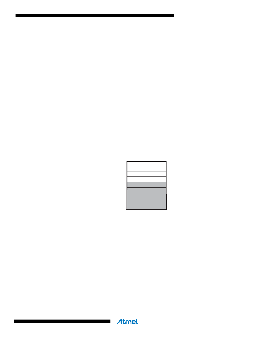
The lower 768 data memory locations address both the Register File, the I/O memory, Extended
I/O memory, and the internal data SRAM. The first 32 locations address the Register File, the
next 64 location the standard I/O memory, then 160 locations of Extended I/O memory, and the
next 512 locations address the internal data SRAM.
The five different addressing modes for the data memory cover: Direct, Indirect with Displace-
ment, Indirect, Indirect with Pre-decrement, and Indirect with Post-increment. In the Register
File, registers R26 to R31 feature the indirect addressing pointer registers.
The direct addressing reaches the entire data space.
The Indirect with Displacement mode reaches 63 address locations from the base address given
by the Y- or Z-register.
When using register indirect addressing modes with automatic pre-decrement and post-incre-
ment, the address registers X, Y, and Z are decremented or incremented.
The 32 general purpose working registers, 64 I/O Registers, 160 Extended I/O Registers, and
the 512 bytes of internal data SRAM in the AT90PWM2/2B/3/3B are all accessible through all
these addressing modes. The Register File is described in “General Purpose Register File” on
Figure 6-2.
Data Memory Map
6.2.1
SRAM Data Access Times
This section describes the general access timing concepts for internal memory access. The
internal data SRAM access is performed in two clk
CPU cycles as described in Figure 6-3.
32 Registers
64 I/O Registers
Internal SRAM
(512 x 8)
0x0000 - 0x001F
0x0020 - 0x005F
0x02FF
0x0060 - 0x00FF
Data Memory
160 Ext I/O Reg.
0x0100
相关PDF资料 |
PDF描述 |
|---|---|
| EP20K100BI324-1 | LOADABLE PLD, PBGA324 |
| EP20K100BI324-2 | LOADABLE PLD, PBGA324 |
| EP20K100BI324-3 | LOADABLE PLD, PBGA324 |
| EP20K100BC484-1 | LOADABLE PLD, PBGA484 |
| EP20K100BC484-2 | LOADABLE PLD, PBGA484 |
相关代理商/技术参数 |
参数描述 |
|---|---|
| EP20K100BC356-1 | 功能描述:FPGA - 现场可编程门阵列 CPLD - APEX 20K 416 Macro 252 IOs RoHS:否 制造商:Altera Corporation 系列:Cyclone V E 栅极数量: 逻辑块数量:943 内嵌式块RAM - EBR:1956 kbit 输入/输出端数量:128 最大工作频率:800 MHz 工作电源电压:1.1 V 最大工作温度:+ 70 C 安装风格:SMD/SMT 封装 / 箱体:FBGA-256 |
| EP20K100BC356-1ES | 制造商:未知厂家 制造商全称:未知厂家 功能描述:FPGA |
| EP20K100BC356-1V | 制造商:Rochester Electronics LLC 功能描述:- Bulk |
| EP20K100BC356-2 | 功能描述:FPGA - 现场可编程门阵列 CPLD - APEX 20K 416 Macro 252 IOs RoHS:否 制造商:Altera Corporation 系列:Cyclone V E 栅极数量: 逻辑块数量:943 内嵌式块RAM - EBR:1956 kbit 输入/输出端数量:128 最大工作频率:800 MHz 工作电源电压:1.1 V 最大工作温度:+ 70 C 安装风格:SMD/SMT 封装 / 箱体:FBGA-256 |
| EP20K100BC356-2ES | 制造商:未知厂家 制造商全称:未知厂家 功能描述:FPGA |
发布紧急采购,3分钟左右您将得到回复。