- 您现在的位置:买卖IC网 > PDF目录299030 > EP20K100BC324-3 (ALTERA CORP) LOADABLE PLD, PBGA324 PDF资料下载
参数资料
| 型号: | EP20K100BC324-3 |
| 厂商: | ALTERA CORP |
| 元件分类: | PLD |
| 英文描述: | LOADABLE PLD, PBGA324 |
| 文件页数: | 7/68页 |
| 文件大小: | 975K |
| 代理商: | EP20K100BC324-3 |
第1页第2页第3页第4页第5页第6页当前第7页第8页第9页第10页第11页第12页第13页第14页第15页第16页第17页第18页第19页第20页第21页第22页第23页第24页第25页第26页第27页第28页第29页第30页第31页第32页第33页第34页第35页第36页第37页第38页第39页第40页第41页第42页第43页第44页第45页第46页第47页第48页第49页第50页第51页第52页第53页第54页第55页第56页第57页第58页第59页第60页第61页第62页第63页第64页第65页第66页第67页第68页
15
4317K–AVR–03/2013
AT90PWM2/3/2B/3B
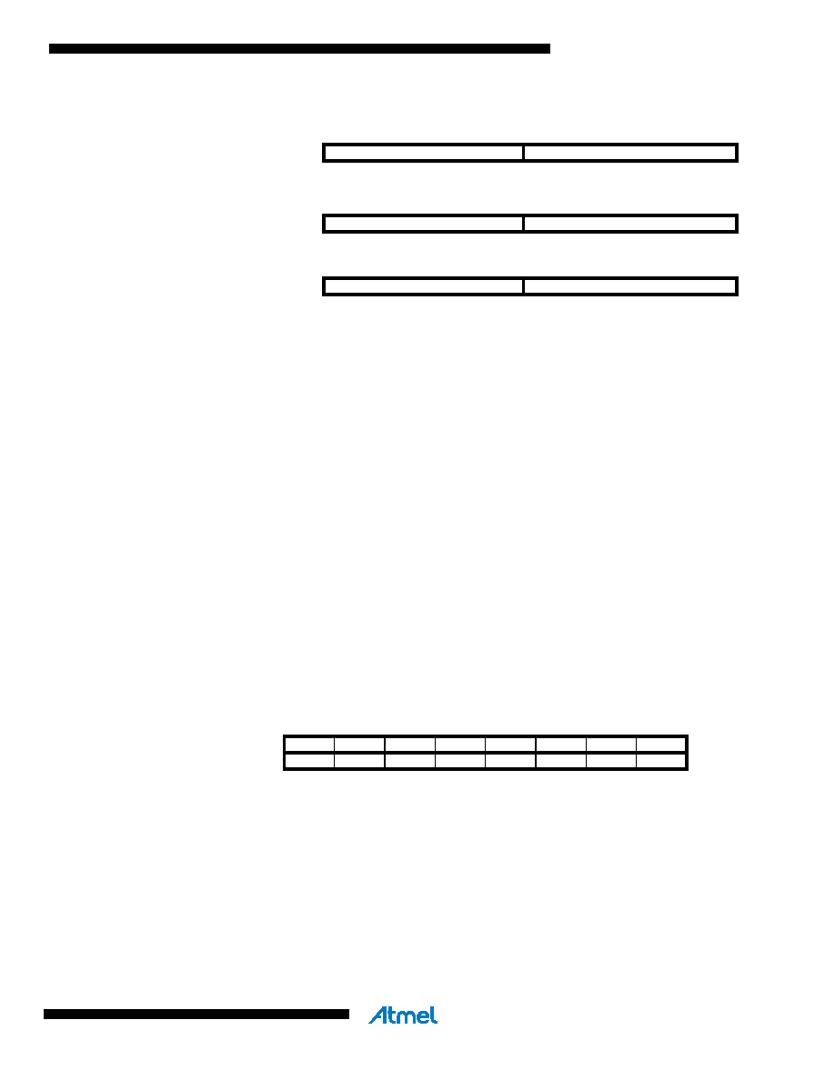
Figure 5-3.
The X-, Y-, and Z-registers
In the different addressing modes these address registers have functions as fixed displacement,
automatic increment, and automatic decrement (see the instruction set reference for details).
5.6
Stack Pointer
The Stack is mainly used for storing temporary data, for storing local variables and for storing
return addresses after interrupts and subroutine calls. The Stack Pointer Register always points
to the top of the Stack. Note that the Stack is implemented as growing from higher memory loca-
tions to lower memory locations. This implies that a Stack PUSH command decreases the Stack
Pointer.
The Stack Pointer points to the data SRAM Stack area where the Subroutine and Interrupt
Stacks are located. This Stack space in the data SRAM must be defined by the program before
any subroutine calls are executed or interrupts are enabled. The Stack Pointer must be set to
point above 0x100. The Stack Pointer is decremented by one when data is pushed onto the
Stack with the PUSH instruction, and it is decremented by two when the return address is
pushed onto the Stack with subroutine call or interrupt. The Stack Pointer is incremented by one
when data is popped from the Stack with the POP instruction, and it is incremented by two when
data is popped from the Stack with return from subroutine RET or return from interrupt RETI.
The AVR Stack Pointer is implemented as two 8-bit registers in the I/O space. The number of
bits actually used is implementation dependent. Note that the data space in some implementa-
tions of the AVR architecture is so small that only SPL is needed. In this case, the SPH Register
will not be present.
5.7
Instruction Execution Timing
This section describes the general access timing concepts for instruction execution. The AVR
CPU is driven by the CPU clock clk
CPU, directly generated from the selected clock source for the
chip. No internal clock division is used.
15
XH
XL
0
X-register
70
7
0
R27 (0x1B)
R26 (0x1A)
15
YH
YL
0
Y-register
70
7
0
R29 (0x1D)
R28 (0x1C)
15
ZH
ZL
0
Z-register
70
7
0
R31 (0x1F)
R30 (0x1E)
Bit
15141312
1110
9
8
SP15
SP14
SP13
SP12
SP11
SP10
SP9
SP8
SPH
SP7
SP6
SP5
SP4
SP3
SP2
SP1
SP0
SPL
7
6543
21
0
Read/Write
R/W
Initial Value
0
0000
00
0
0000
00
0
相关PDF资料 |
PDF描述 |
|---|---|
| EP20K100BI324-1 | LOADABLE PLD, PBGA324 |
| EP20K100BI324-2 | LOADABLE PLD, PBGA324 |
| EP20K100BI324-3 | LOADABLE PLD, PBGA324 |
| EP20K100BC484-1 | LOADABLE PLD, PBGA484 |
| EP20K100BC484-2 | LOADABLE PLD, PBGA484 |
相关代理商/技术参数 |
参数描述 |
|---|---|
| EP20K100BC356-1 | 功能描述:FPGA - 现场可编程门阵列 CPLD - APEX 20K 416 Macro 252 IOs RoHS:否 制造商:Altera Corporation 系列:Cyclone V E 栅极数量: 逻辑块数量:943 内嵌式块RAM - EBR:1956 kbit 输入/输出端数量:128 最大工作频率:800 MHz 工作电源电压:1.1 V 最大工作温度:+ 70 C 安装风格:SMD/SMT 封装 / 箱体:FBGA-256 |
| EP20K100BC356-1ES | 制造商:未知厂家 制造商全称:未知厂家 功能描述:FPGA |
| EP20K100BC356-1V | 制造商:Rochester Electronics LLC 功能描述:- Bulk |
| EP20K100BC356-2 | 功能描述:FPGA - 现场可编程门阵列 CPLD - APEX 20K 416 Macro 252 IOs RoHS:否 制造商:Altera Corporation 系列:Cyclone V E 栅极数量: 逻辑块数量:943 内嵌式块RAM - EBR:1956 kbit 输入/输出端数量:128 最大工作频率:800 MHz 工作电源电压:1.1 V 最大工作温度:+ 70 C 安装风格:SMD/SMT 封装 / 箱体:FBGA-256 |
| EP20K100BC356-2ES | 制造商:未知厂家 制造商全称:未知厂家 功能描述:FPGA |
发布紧急采购,3分钟左右您将得到回复。