- 您现在的位置:买卖IC网 > PDF目录97926 > EPF10K200S Programmable Logic PDF资料下载
参数资料
| 型号: | EPF10K200S |
| 英文描述: | Programmable Logic |
| 中文描述: | 可编程逻辑 |
| 文件页数: | 70/138页 |
| 文件大小: | 2116K |
| 代理商: | EPF10K200S |
第1页第2页第3页第4页第5页第6页第7页第8页第9页第10页第11页第12页第13页第14页第15页第16页第17页第18页第19页第20页第21页第22页第23页第24页第25页第26页第27页第28页第29页第30页第31页第32页第33页第34页第35页第36页第37页第38页第39页第40页第41页第42页第43页第44页第45页第46页第47页第48页第49页第50页第51页第52页第53页第54页第55页第56页第57页第58页第59页第60页第61页第62页第63页第64页第65页第66页第67页第68页第69页当前第70页第71页第72页第73页第74页第75页第76页第77页第78页第79页第80页第81页第82页第83页第84页第85页第86页第87页第88页第89页第90页第91页第92页第93页第94页第95页第96页第97页第98页第99页第100页第101页第102页第103页第104页第105页第106页第107页第108页第109页第110页第111页第112页第113页第114页第115页第116页第117页第118页第119页第120页第121页第122页第123页第124页第125页第126页第127页第128页第129页第130页第131页第132页第133页第134页第135页第136页第137页第138页
Altera Corporation
37
FLEX 10K Embedded Programmable Logic Family Data Sheet
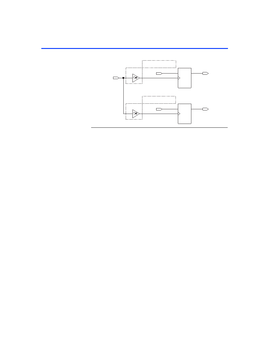
Figure 17. Enabling ClockLock & ClockBoost in the Same Design
To use both the ClockLock and ClockBoost circuits in the same design,
designers must use Revision C EPF10K100GC503-3DX devices and
MAX+PLUS II software versions 7.2 or higher. The die revision is
indicated by the third digit of the nine-digit code on the top side of the
device.
f For more information on using the ClockLock and ClockBoost features,
see the Clock Management with ClockLock & ClockBoost Features White Paper,
which is available from Altera Literature Services.
Output
Conguration
This section discusses the peripheral component interconnect (PCI)
pull-up clamping diode option, slew-rate control, open-drain output
option, MultiVolt I/O interface, and power sequencing for FLEX 10K
devices. The PCI pull-up clamping diode, slew-rate control, and
open-drain output options are controlled pin-by-pin via MAX+PLUS II
logic options. The MultiVolt I/O interface is controlled by connecting
VCCIO to a different voltage than VCCINT. Its effect can be simulated in the
MAX+PLUS II software via the Global Project Device Options dialog
box (Assign menu).
PCI Clamping Diodes
The EPF10K10A and EPF10K30A devices have a pull-up clamping diode
on every I/O, dedicated input, and dedicated clock pin. PCI clamping
diodes clamp the transient overshoot caused by reflected waves to the
VCCIO value and are required for 3.3-V PCI compliance. Clamping diodes
can also be used to limit overshoot in other systems.
D
Q
D
Q
a
b
aout
bout
gclk1
CLKLOCK
CLOCKBOOST=1
INPUT_FREQUENCY=50
CLOCKBOOST=2
INPUT_FREQUENCY=50
相关PDF资料 |
PDF描述 |
|---|---|
| EPF10K130EFC484-3 | Field Programmable Gate Array (FPGA) |
| EPF10K130EFC672-1 | Field Programmable Gate Array (FPGA) |
| EPF10K130EFC672-1X | Field Programmable Gate Array (FPGA) |
| EPF10K130EFC672-2 | Field Programmable Gate Array (FPGA) |
| EPF10K200EBC600-2 | Field Programmable Gate Array (FPGA) |
相关代理商/技术参数 |
参数描述 |
|---|---|
| EPF10K200SBC356-1 | 功能描述:FPGA - 现场可编程门阵列 FPGA - Flex 10K 1248 LABs 274 IOs RoHS:否 制造商:Altera Corporation 系列:Cyclone V E 栅极数量: 逻辑块数量:943 内嵌式块RAM - EBR:1956 kbit 输入/输出端数量:128 最大工作频率:800 MHz 工作电源电压:1.1 V 最大工作温度:+ 70 C 安装风格:SMD/SMT 封装 / 箱体:FBGA-256 |
| EPF10K200SBC356-1X | 功能描述:FPGA - 现场可编程门阵列 FPGA - Flex 10K 1248 LABs 274 IOs RoHS:否 制造商:Altera Corporation 系列:Cyclone V E 栅极数量: 逻辑块数量:943 内嵌式块RAM - EBR:1956 kbit 输入/输出端数量:128 最大工作频率:800 MHz 工作电源电压:1.1 V 最大工作温度:+ 70 C 安装风格:SMD/SMT 封装 / 箱体:FBGA-256 |
| EPF10K200SBC356-2 | 功能描述:FPGA - 现场可编程门阵列 FPGA - Flex 10K 1248 LABs 274 IOs RoHS:否 制造商:Altera Corporation 系列:Cyclone V E 栅极数量: 逻辑块数量:943 内嵌式块RAM - EBR:1956 kbit 输入/输出端数量:128 最大工作频率:800 MHz 工作电源电压:1.1 V 最大工作温度:+ 70 C 安装风格:SMD/SMT 封装 / 箱体:FBGA-256 |
| EPF10K200SBC356-2X | 功能描述:FPGA - 现场可编程门阵列 FPGA - Flex 10K 1248 LABs 274 IOs RoHS:否 制造商:Altera Corporation 系列:Cyclone V E 栅极数量: 逻辑块数量:943 内嵌式块RAM - EBR:1956 kbit 输入/输出端数量:128 最大工作频率:800 MHz 工作电源电压:1.1 V 最大工作温度:+ 70 C 安装风格:SMD/SMT 封装 / 箱体:FBGA-256 |
| EPF10K200SBC356-3 | 功能描述:FPGA - 现场可编程门阵列 FPGA - Flex 10K 1248 LABs 274 IOs RoHS:否 制造商:Altera Corporation 系列:Cyclone V E 栅极数量: 逻辑块数量:943 内嵌式块RAM - EBR:1956 kbit 输入/输出端数量:128 最大工作频率:800 MHz 工作电源电压:1.1 V 最大工作温度:+ 70 C 安装风格:SMD/SMT 封装 / 箱体:FBGA-256 |
发布紧急采购,3分钟左右您将得到回复。