- 您现在的位置:买卖IC网 > PDF目录16441 > EVAL-AD9880-ABZ (Analog Devices Inc)KIT MODULE VIDEO INPUT AD9880 PDF资料下载
参数资料
| 型号: | EVAL-AD9880-ABZ |
| 厂商: | Analog Devices Inc |
| 文件页数: | 6/64页 |
| 文件大小: | 0K |
| 描述: | KIT MODULE VIDEO INPUT AD9880 |
| 标准包装: | 1 |
| 主要目的: | 视频,视频处理 |
| 嵌入式: | 否 |
| 已用 IC / 零件: | AD9880 |
| 主要属性: | HDMI 接收器和模拟接口 |
| 次要属性: | 3 路 8 位 150MSPS ADC |
| 已供物品: | 板 |
第1页第2页第3页第4页第5页当前第6页第7页第8页第9页第10页第11页第12页第13页第14页第15页第16页第17页第18页第19页第20页第21页第22页第23页第24页第25页第26页第27页第28页第29页第30页第31页第32页第33页第34页第35页第36页第37页第38页第39页第40页第41页第42页第43页第44页第45页第46页第47页第48页第49页第50页第51页第52页第53页第54页第55页第56页第57页第58页第59页第60页第61页第62页第63页第64页
AD9880
Rev. 0 | Page 14 of 64
required. Note that the SOG signal is always negative polarity.
For additional detail on setting the SOG threshold and other
SOG-related functions, see the Sync Processing section.
05087-004
GAIN
SOG
1nF
RAIN
47nF
BAIN
47nF
Figure 4. Typical Clamp Configuration for RGB/YUV Applications
Clock Generation
A PLL is employed to generate the pixel clock. In this PLL,
the Hsync input provides a reference frequency. A voltage
controlled oscillator (VCO) generates a much higher pixel clock
frequency. This pixel clock is divided by the PLL divide value
(Registers 0x01 and 0x02) and phase compared with the Hsync
input. Any error is used to shift the VCO frequency and
maintain lock between the two signals.
The stability of this clock is a very important element in provi-
ding the clearest and most stable image. During each pixel time,
there is a period during which the signal slews from the old
pixel amplitude and settles at its new value. This is followed by a
time when the input voltage is stable before the signal must slew
to a new value. The ratio of the slewing time to the stable time is
a function of the bandwidth of the graphics DAC and the
bandwidth of the transmission system (cable and termination).
It is also a function of the overall pixel rate. Clearly, if the
dynamic characteristics of the system remain fixed, then the
slewing and settling time is likewise fixed. This time must be
subtracted from the total pixel period, leaving the stable period.
At higher pixel frequencies, the total cycle time is shorter and
the stable pixel time also becomes shorter.
PIXEL CLOCK
INVALID SAMPLE TIMES
05087-005
Figure 5. Pixel Sampling Times
Any jitter in the clock reduces the precision with which the
sampling time can be determined and must also be subtracted
from the stable pixel time. Considerable care has been taken in
the design of the AD9880’s clock generation circuit to minimize
jitter. The clock jitter of the AD9880 is less than 13% of the total
pixel time in all operating modes, making the reduction in the
valid sampling time due to jitter negligible.
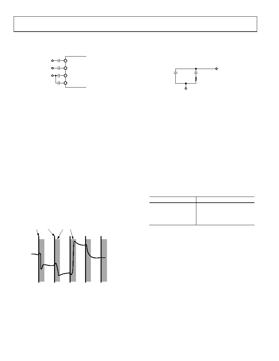
The PLL characteristics are determined by the loop filter design,
the PLL charge pump current, and the VCO range setting. The
loop filter design is illustrated in Figure 6. Recommended set-
tings of the VCO range and charge pump current for VESA
standard display modes are listed in Table 8.
CP
8nF
CZ
80nF
RZ
1.5k
Ω
FILT
PVD
05087-006
Figure 6. PLL Loop Filter Detail
Four programmable registers are provided to optimize the
performance of the PLL. These registers are
The 12-Bit Divisor Register. The input Hsync frequency
range can be any frequency which, combined with the
PLL_Div, does not exceed the VCO range . The PLL multi-
plies the frequency of the Hsync signal, producing pixel
clock frequencies in the range of 10 MHz to 100 MHz. The
divisor register controls the exact multiplication factor.
The 2-Bit VCO Range Register. To improve the noise
performance of the AD9880, the VCO operating frequency
range is divided into four overlapping regions. The VCO
range register sets this operating range. The frequency
ranges for the lowest and highest regions are shown in
Table 6.
VCORNGE
Pixel Rate Range
00
12-30
01
30-60
10
60-120
11
120-150
The 5-Bit Phase Adjust Register. The phase of the
generated sampling clock can be shifted to locate an
optimum sampling point within a clock cycle. The phase
adjust register provides 32 phase-shift steps of 11.25° each.
The Hsync signal with an identical phase shift is available
through the HSOUT pin.
The COAST pin or the internal Coast is used to allow the PLL
to continue to run at the same frequency, in the absence of the
incoming Hsync signal or during disturbances in Hsync (such
as equalization pulses). This can be used during the vertical
sync period or any other time that the Hsync signal is unavail-
able. The polarity of the Coast signal can be set through the
Coast polarity register. Also, the polarity of the Hsync signal
can be set through the Hsync polarity register. For both Hsync
and Coast, a value of 1 is active high. The internal Coast
function is driven off the Vsync signal, which is typically a time
when Hsync signals can be disrupted with extra equalization
pulses.
相关PDF资料 |
PDF描述 |
|---|---|
| EVAL-ADV7611EB2Z | BOARD EVALUATION FOR ADV7611 |
| 1-1906012-2 | CA 2.0MM OFNR 50/125,LC SEC RED |
| 4922R-17L | INDUCTOR 22UH POWER SMD |
| GMM12DTAD | CONN EDGECARD 24POS R/A .156 SLD |
| S200-2-W1-22-9 | SOLDERSLEEVE SHLD TERMI W/LEADS |
相关代理商/技术参数 |
参数描述 |
|---|---|
| EVAL-ADAS1000EBZU1 | 功能描述:EVAL BOARD ADAS1000 ECG AFE RoHS:是 类别:编程器,开发系统 >> 评估演示板和套件 系列:* 产品培训模块:Obsolescence Mitigation Program 标准包装:1 系列:- 主要目的:电源管理,电池充电器 嵌入式:否 已用 IC / 零件:MAX8903A 主要属性:1 芯锂离子电池 次要属性:状态 LED 已供物品:板 |
| EVAL-ADAS1000SDZ | 功能描述:数据转换 IC 开发工具 EVALUATION BOARD RoHS:否 制造商:Texas Instruments 产品:Demonstration Kits 类型:ADC 工具用于评估:ADS130E08 接口类型:SPI 工作电源电压:- 6 V to + 6 V |
| EVAL-ADAS1000SDZU3 | 制造商:Analog Devices 功能描述:EVALUATION KIT - Boxed Product (Development Kits) |
| EVAL-ADAS1000SDZU4 | 制造商:Analog Devices 功能描述:EVAL BOARD ANAS1000 ECG AFE |
| EVAL-ADAS1127CBZ | 功能描述:BOARD EVAL FOR ADAS1127 RoHS:是 类别:编程器,开发系统 >> 评估板 - 模数转换器 (ADC) 系列:* 产品培训模块:Obsolescence Mitigation Program 标准包装:1 系列:- ADC 的数量:1 位数:12 采样率(每秒):94.4k 数据接口:USB 输入范围:±VREF/2 在以下条件下的电源(标准):- 工作温度:-40°C ~ 85°C 已用 IC / 零件:MAX11645 已供物品:板,软件 |
发布紧急采购,3分钟左右您将得到回复。