- 您现在的位置:买卖IC网 > PDF目录375778 > FDB13AN06A0 (FAIRCHILD SEMICONDUCTOR CORP) N-Channel PowerTrench MOSFET 60V, 62A, 13.5mohm PDF资料下载
参数资料
| 型号: | FDB13AN06A0 |
| 厂商: | FAIRCHILD SEMICONDUCTOR CORP |
| 元件分类: | JFETs |
| 英文描述: | N-Channel PowerTrench MOSFET 60V, 62A, 13.5mohm |
| 中文描述: | 62 A, 60 V, 0.0135 ohm, N-CHANNEL, Si, POWER, MOSFET, TO-263AB |
| 封装: | TO-263AB, 3 PIN |
| 文件页数: | 7/11页 |
| 文件大小: | 300K |
| 代理商: | FDB13AN06A0 |
2003 Fairchild Semiconductor Corporation
FDB13AN06A0 / FDP13AN06A0 Rev. A1
F
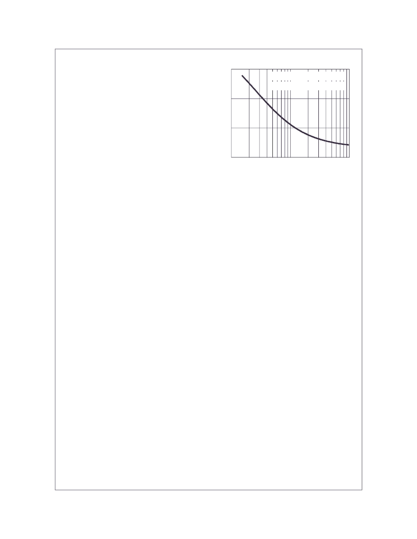
Thermal Resistance vs. Mounting Pad Area
The maximum rated junction temperature, T
JM
, and the
thermal resistance of the heat dissipating path determines
the maximum allowable device power dissipation, P
DM
, in an
application.
Therefore
temperature, T
A
(
o
C), and thermal resistance R
θ
JA
(
o
C/W)
must be reviewed to ensure that T
JM
is never exceeded.
Equation 1 mathematically represents the relationship and
serves as the basis for establishing the rating of the part.
the
application
’
s
ambient
In using surface mount devices such as the TO-263
package, the environment in which it is applied will have a
significant influence on the part
’
s current and maximum
power dissipation ratings. Precise determination of P
DM
is
complex and influenced by many factors:
1. Mounting pad area onto which the device is attached and
whether there is copper on one side or both sides of the
board.
2. The number of copper layers and the thickness of the
board.
3. The use of external heat sinks.
4. The use of thermal vias.
5. Air flow and board orientation.
6. For non steady state applications, the pulse width, the
duty cycle and the transient thermal response of the part,
the board and the environment they are in.
Fairchild provides thermal information to assist the
designer
’
s preliminary application evaluation. Figure 21
defines the R
θ
JA
for the device as a function of the top
copper (component side) area. This is for a horizontally
positioned FR-4 board with 1oz copper after 1000 seconds
of steady state power with no air flow. This graph provides
the necessary information for calculation of the steady state
junction
temperature
or
applications can be evaluated using the Fairchild device
Spice thermal model or manually utilizing the normalized
maximum transient thermal impedance curve.
power
dissipation.
Pulse
Thermal resistances corresponding to other copper areas
can be obtained from Figure 21 or by calculation using
Equation 2 or 3. Equation 2 is used for copper area defined
in inches square and equation 3 is for area in centimeters
square. The area, in square inches or square centimeters is
the top copper area including the gate and source pads.
(EQ. 1)
PDM
θ
JA
–
(
-----------------------------
)
=
Area in Inches Squared
(EQ. 2)
R
θ
JA
26.51
+
0.262
Area
(
)
-----------19.84
+
=
(EQ. 3)
R
θ
JA
26.51
+
1.69
Area
(
)
-----------128
+
=
Area in Centimeters Squared
Figure 21. Thermal Resistance vs Mounting
Pad Area
20
40
60
80
1
10
0.1
R
θ
JA
= 26.51+ 19.84/(0.262+Area) EQ.2
R
θ
J
(
o
C
AREA, TOP COPPER AREA in
2
(cm
2
)
(0.645)
(6.45)
(64.5)
R
θ
JA
= 26.51+ 128/(1.69+Area) EQ.3
相关PDF资料 |
PDF描述 |
|---|---|
| FDP13AN06A0 | N-Channel PowerTrench MOSFET 60V, 62A, 13.5mз |
| FDP14N30 | 300V N-Channel MOSFET |
| FDPF14N30 | 300V N-Channel MOSFET |
| FDP15N65_0610 | 650V N-Channel MOSFET |
| FDP15N65 | 650V N-Channel MOSFET |
相关代理商/技术参数 |
参数描述 |
|---|---|
| FDB13AN06A0_Q | 功能描述:MOSFET N-Channel PowerTrench RoHS:否 制造商:STMicroelectronics 晶体管极性:N-Channel 汲极/源极击穿电压:650 V 闸/源击穿电压:25 V 漏极连续电流:130 A 电阻汲极/源极 RDS(导通):0.014 Ohms 配置:Single 最大工作温度: 安装风格:Through Hole 封装 / 箱体:Max247 封装:Tube |
| FDB14AN06L_F085 | 制造商:FAIRCHILD 制造商全称:Fairchild Semiconductor 功能描述:N-Channel PowerTrench?? MOSFET 60V, 60A, 14.6mW |
| FDB14AN06LA0 | 功能描述:MOSFET 60V N-Ch PowerTrench MOSFET RoHS:否 制造商:STMicroelectronics 晶体管极性:N-Channel 汲极/源极击穿电压:650 V 闸/源击穿电压:25 V 漏极连续电流:130 A 电阻汲极/源极 RDS(导通):0.014 Ohms 配置:Single 最大工作温度: 安装风格:Through Hole 封装 / 箱体:Max247 封装:Tube |
| FDB14AN06LA0_F085 | 功能描述:MOSFET 60V N-CHAN PwrTrench RoHS:否 制造商:STMicroelectronics 晶体管极性:N-Channel 汲极/源极击穿电压:650 V 闸/源击穿电压:25 V 漏极连续电流:130 A 电阻汲极/源极 RDS(导通):0.014 Ohms 配置:Single 最大工作温度: 安装风格:Through Hole 封装 / 箱体:Max247 封装:Tube |
| FDB14N30 | 制造商:FAIRCHILD 制造商全称:Fairchild Semiconductor 功能描述:300V N-Channel MOSFET |
发布紧急采购,3分钟左右您将得到回复。