- 您现在的位置:买卖IC网 > Datasheet目录424 > FDP8030L (Fairchild Semiconductor)MOSFET N-CH 30V 80A TO220 Datasheet资料下载
参数资料
| 型号: | FDP8030L |
| 厂商: | Fairchild Semiconductor |
| 文件页数: | 2/5页 |
| 文件大小: | 0K |
| 描述: | MOSFET N-CH 30V 80A TO220 |
| 产品培训模块: | High Voltage Switches for Power Processing |
| 标准包装: | 50 |
| 系列: | PowerTrench® |
| FET 型: | MOSFET N 通道,金属氧化物 |
| FET 特点: | 逻辑电平门 |
| 漏极至源极电压(Vdss): | 30V |
| 电流 - 连续漏极(Id) @ 25° C: | 80A |
| 开态Rds(最大)@ Id, Vgs @ 25° C: | 3.5 毫欧 @ 80A,10V |
| Id 时的 Vgs(th)(最大): | 2V @ 250µA |
| 闸电荷(Qg) @ Vgs: | 170nC @ 5V |
| 输入电容 (Ciss) @ Vds: | 10500pF @ 15V |
| 功率 - 最大: | 187W |
| 安装类型: | 通孔 |
| 封装/外壳: | TO-220-3 |
| 供应商设备封装: | TO-220 |
| 包装: | 管件 |
| 其它名称: | FDP8030L-ND FDP8030LFS |
�� �
�
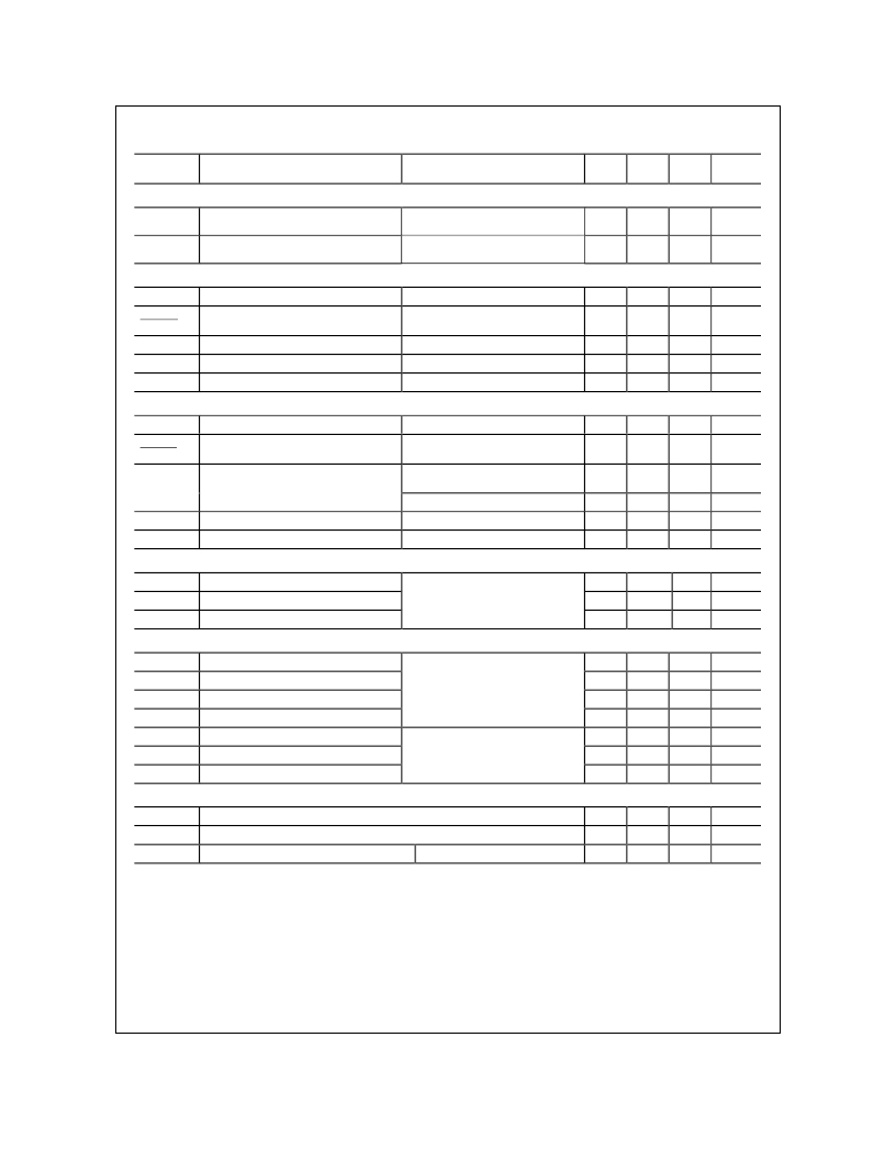
�Electrical� Characteristics�
�T� A� =� 25°C� unless� otherwise� noted�
�Symbol�
�Parameter�
�Test� Conditions�
�Min�
�Typ�
�Max� Units�
�Drain-Source� Avalanche� Ratings� (Note� 1)�
�W� DSS�
�Single� Pulse� Drain-Source�
�V� DD� =� 20� V,�
�I� D� =� 80� A�
�1500�
�mJ�
�Avalanche� Energy�
�I� AR�
�Maximum� Drain-Source� Avalanche�
�80�
�A�
�Current�
�Off� Characteristics�
�BV� DSS�
�?� BV� DSS�
�?� T� J�
�Drain–Source� Breakdown� Voltage�
�Breakdown� Voltage� Temperature�
�Coefficient�
�V� GS� =� 0� V,� I� D� =� 250� μ� A�
�I� D� =� 250� μ� A,� Referenced� to� 25� °� C�
�30�
�23�
�V�
�mV/� °� C�
�I� DSS�
�I� GSSF�
�I� GSSR�
�Zero� Gate� Voltage� Drain� Current�
�Gate–Body� Leakage,� Forward�
�Gate–Body� Leakage,� Reverse�
�V� DS� =� 24� V,�
�V� GS� =� 20� V,�
�V� GS� =� –20� V�
�V� GS� =� 0� V�
�V� DS� =� 0� V�
�V� DS� =� 0� V�
�10�
�100�
�–100�
�μ� A�
�nA�
�nA�
�On� Characteristics�
�(Note� 2)�
�V� GS(th)�
�?� V� GS(th)�
�?� T� J�
�Gate� Threshold� Voltage�
�Gate� Threshold� Voltage�
�Temperature� Coefficient�
�V� DS� =� V� GS� ,� I� D� =� 250� μ� A�
�I� D� =� 250� μ� A,� Referenced� to� 25� °� C�
�1�
�1.5�
�–5�
�2�
�V�
�mV/� °� C�
�R� DS(on)�
�Static� Drain–Source�
�On–Resistance�
�V� GS� =� 10� V,�
�I� D� =� 80� A�
�T� J� =125� °� C�
�3.1�
�4.0�
�3.5�
�5.6�
�m� ?�
�V� GS� =� 4.5� V,�
�I� D� =� 70� A�
�3.6�
�4.5�
�I� D(on)�
�g� FS�
�On–State� Drain� Current�
�Forward� Transconductance�
�V� GS� =� 10� V,�
�V� DS� =� 10� V,�
�V� DS� =� 10� V�
�I� D� =� 80� A�
�60�
�170�
�A�
�S�
�Dynamic� Characteristics�
�C� iss�
�C� oss�
�C� rss�
�Input� Capacitance�
�Output� Capacitance�
�Reverse� Transfer� Capacitance�
�V� DS� =� 15� V,�
�f� =� 1.0� MHz�
�V� GS� =� 0� V,�
�10500�
�2700�
�1650�
�pF�
�pF�
�pF�
�Switching� Characteristics�
�(Note� 2)�
�t� D(on)�
�t� r�
�t� D� (off)�
�t� f�
�Q� g�
�Turn–On� Delay� Time�
�Turn–On� Rise� Time�
�Turn–Off� Delay� Time�
�Turn–Off� Fall� Time�
�Total� Gate� Charge�
�V� DD� =� 15� V,�
�V� GS� =� 4.5� V,�
�R� GS� =� 10� ?�
�V� DS� =� 15� V,�
�I� D� =� 50� A,�
�R� GEN� =� 10� ?�
�20�
�185�
�160�
�200�
�120�
�35�
�225�
�200�
�240�
�170�
�ns�
�ns�
�ns�
�ns�
�nC�
�Q� gs�
�Q� gd�
�Gate–Source� Charge�
�Gate–Drain� Charge�
�I� D� =� 80� A,� V� GS� =� 5� V�
�27�
�48�
�nC�
�nC�
�Drain–Source� Diode� Characteristics� and� Maximum� Ratings�
�I� S�
�I� SM�
�Maximum� Continuous� Drain–Source� Diode� Forward� Current�
�Maximum� Pulsed� Drain-Source� Diode� Forward� Current�
�(Note� 1)�
�(Note� 1)�
�80�
�300�
�A�
�A�
�V� SD�
�Drain–Source� Diode� Forward� Voltage�
�V� GS� =� 0� V,�
�I� S� =� 80� A�
�(Note� 1)�
�1�
�1.3�
�V�
�Notes:�
�1.� Pulse� Test:� Pulse� Width� <� 300� μ� s,� Duty� Cycle� <� 2.0%�
�FDP8030L/FDB8030L� Rev� C2(W)�
�相关PDF资料 |
PDF描述 |
|---|---|
| FDP80N06 | MOSFET N-CH 60V 80A TO-220 |
| FDP8440 | MOSFET N-CH 40V 100A TO-220 |
| FDP8441 | MOSFET N-CH 40V 80A TO-220AB |
| FDP8443_F085 | MOSFET N-CH 40V TO-220AB-3 |
| FDP8447L | MOSFET N-CH 40V 12A TO-220 |
相关代理商/技术参数 |
参数描述 |
|---|---|
| FDP8030L_Q | 功能描述:MOSFET N-Ch PowerTrench Logic Level RoHS:否 制造商:STMicroelectronics 晶体管极性:N-Channel 汲极/源极击穿电压:650 V 闸/源击穿电压:25 V 漏极连续电流:130 A 电阻汲极/源极 RDS(导通):0.014 Ohms 配置:Single 最大工作温度: 安装风格:Through Hole 封装 / 箱体:Max247 封装:Tube |
| FDP80N06 | 功能描述:MOSFET 60V N-Channel RoHS:否 制造商:STMicroelectronics 晶体管极性:N-Channel 汲极/源极击穿电压:650 V 闸/源击穿电压:25 V 漏极连续电流:130 A 电阻汲极/源极 RDS(导通):0.014 Ohms 配置:Single 最大工作温度: 安装风格:Through Hole 封装 / 箱体:Max247 封装:Tube |
| FDP8440 | 功能描述:MOSFET 40V N-Channel Power Trench RoHS:否 制造商:STMicroelectronics 晶体管极性:N-Channel 汲极/源极击穿电压:650 V 闸/源击穿电压:25 V 漏极连续电流:130 A 电阻汲极/源极 RDS(导通):0.014 Ohms 配置:Single 最大工作温度: 安装风格:Through Hole 封装 / 箱体:Max247 封装:Tube |
| FDP8441 | 功能描述:MOSFET 40V N-Channel PowerTrench MOSFET RoHS:否 制造商:STMicroelectronics 晶体管极性:N-Channel 汲极/源极击穿电压:650 V 闸/源击穿电压:25 V 漏极连续电流:130 A 电阻汲极/源极 RDS(导通):0.014 Ohms 配置:Single 最大工作温度: 安装风格:Through Hole 封装 / 箱体:Max247 封装:Tube |
| FDP8441_F085 | 功能描述:MOSFET 40V N-Ch PowerTrench RoHS:否 制造商:STMicroelectronics 晶体管极性:N-Channel 汲极/源极击穿电压:650 V 闸/源击穿电压:25 V 漏极连续电流:130 A 电阻汲极/源极 RDS(导通):0.014 Ohms 配置:Single 最大工作温度: 安装风格:Through Hole 封装 / 箱体:Max247 封装:Tube |
发布紧急采购,3分钟左右您将得到回复。