- 您现在的位置:买卖IC网 > Datasheet目录327 > HW-V5-ML555-G (Xilinx Inc)BOARD EVAL FOR VIRTEX-5 ML555 Datasheet资料下载
参数资料
| 型号: | HW-V5-ML555-G |
| 厂商: | Xilinx Inc |
| 文件页数: | 58/108页 |
| 文件大小: | 0K |
| 描述: | BOARD EVAL FOR VIRTEX-5 ML555 |
| 产品培训模块: | PCI Express and Virtex® -5 FPGAs |
| 标准包装: | 1 |
| 系列: | Virtex® -5 |
| 类型: | FPGA |
| 适用于相关产品: | Virtex?-5 FPGA |
| 所含物品: | 板,线缆,CD |
| 配用: | HW-AFX-SMA-SFP-ND - CONVERSION MODULE SMA - SFP HW-AFX-SMA-SATA-ND - CONVERSION MODULE SMA - SATA HW-AFX-SMA-RJ45-ND - CONVERSION MODULE SMA - RJ45 HW-AFX-SMA-HSSDC2-ND - CONVERSION MODULE SMA - HSSDC2 HW-AFX-BERG-EPHY-ND - DAUGHTER CARD PHY BERG-EPHY |
| 相关产品: | XC5VFX70T-1FF1136CES-ND - IC FPGAVIRTEX5FX ES 70K 1136FBGA XC5VLX85T-3FF1136C-ND - IC FPGA VIRTEX-5 85K 1136FBGA XC5VLX85T-2FF1136I-ND - IC FPGA VIRTEX-5 85K 1136FBGA XC5VLX85T-2FF1136C-ND - IC FPGA VIRTEX-5 85K 1136FBGA XC5VLX85T-1FF1136I-ND - IC FPGA VIRTEX-5 85K 1136FBGA XC5VLX85T-1FF1136C-ND - IC FPGA VIRTEX-5 85K 1136FBGA XC5VLX50T-3FF1136C-ND - IC FPGA VIRTEX-5 50K 1136FBGA XC5VLX50T-2FF1136I-ND - IC FPGA VIRTEX-5 50K 1136FBGA XC5VLX50T-2FF1136C-ND - IC FPGA VIRTEX-5 50K 1136FBGA XC5VLX50T-1FF1136I-ND - IC FPGA VIRTEX-5 50K 1136FBGA 更多... |
| 其它名称: | 122-1586 HW-V5-ML555-G-ND |
第1页第2页第3页第4页第5页第6页第7页第8页第9页第10页第11页第12页第13页第14页第15页第16页第17页第18页第19页第20页第21页第22页第23页第24页第25页第26页第27页第28页第29页第30页第31页第32页第33页第34页第35页第36页第37页第38页第39页第40页第41页第42页第43页第44页第45页第46页第47页第48页第49页第50页第51页第52页第53页第54页第55页第56页第57页当前第58页第59页第60页第61页第62页第63页第64页第65页第66页第67页第68页第69页第70页第71页第72页第73页第74页第75页第76页第77页第78页第79页第80页第81页第82页第83页第84页第85页第86页第87页第88页第89页第90页第91页第92页第93页第94页第95页第96页第97页第98页第99页第100页第101页第102页第103页第104页第105页第106页第107页第108页
�� �
�
�Chapter� 3:� Hardware� Description�
�R�
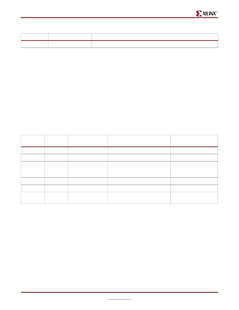
�Table� 3-19:�
�FPGA� Global� Clock� Inputs� (Continued)�
�FPGA� Pins�
�Signal� Name�
�Clock� Source�
�K18,� K19,� H13� No� connects�
�Unused� global� clock� inputs� to� FPGA�
�Notes:�
�1.� AC� coupled.�
�2.� The� SMA� clock� input� can� be� differential� or� single� ended.� When� driven� with� a� single� ended� clock� source,� connector� J10� should� be�
�used� to� input� the� clock� to� the� FPGA.� Differential� clock� inputs� to� the� FPGA� should� use� the� IBUFDS� input� buffer� library� primitive.�
�Setting� the� DIFF_TERM� attribute� of� the� IBUFDS� to� TRUE� provides� 100� Ω� on-chip� termination� for� the� LVDS� clock� source� driver.�
�3.� Single-ended� clock� input.� All� other� clocks� are� differential� inputs.�
�4.� Control� output� port� SATA_MGT_CLKSEL� on� FPGA� pin� H15:�
�(=� 0)� selects� the� fixed� 125� MHz� oscillator� output�
�(=� 1)� selects� the� variable-frequency� Clock� Synthesizer� 2� output�
�as� the� clock� source� for� the� differential� global� clock� inputs� on� FPGA� pins� J20� and� J21.�
�5.� The� SMA� GCLK� ports� can� be� used� as� outputs� to� route� internal� single-ended� or� differential� signals� to� an� oscilloscope� for� debugging�
�ML555� designs.�
�GTP� Reference� Clock� Inputs�
�All� GTP� REFCLK� inputs� have� clock� inputs� routed� to� them.� Table� 3-20� shows� GTP� location�
�designators,� FPGA� pins,� and� clock� sources� that� drive� the� reference� clock� inputs� of� the� GTP�
�transceivers.� The� lanes� are� for� PCI� Express� applications.�
�Table� 3-20:�
�GTP� Reference� Clock� Inputs�
�GTP� LOC�
�Designator�
�X0Y0� (6)�
�X0Y1� (6)�
�X0Y2� (6)�
�FPGA� Pins� (1)�
�AL5,� AL4�
�AF4,� AF3�
�Y4,� Y3�
�Signal� Name� (2)�
�MGT_X0Y0_REFCLK�
�MGT_X0Y1_REFCLK�
�PCIE_REFCLK� (7)�
�Clock� Source� (3,4,5)�
�Clock� Synthesizer� 2�
�Clock� Synthesizer� 1�
�Spread� spectrum� clock� input� from�
�Application� Usage�
�Lanes� 6� and� 7�
�Lanes� 2� and� 3�
�Lanes� 0� and� 1�
�PCI� Express� system� unit� connector�
�P13.� Pins� A13� (P)� and� A14� (N).�
�X0Y3� (6)�
�P4,� P3�
�SMA_GTPCLK�
�SMA� connectors� P12� (P)� and� P13� (N)� Lanes� 4� and� 5�
�X0Y4�
�X0Y5�
�H4,� H3�
�E4,� D4�
�SFP_MGT_REFCLK�
�SATA_MGT_REFCLK�
�125� MHz� Oscillator�
�Selectable:� 125� MHz� Oscillator� or�
�SFP1� and� SFP2� interfaces�
�SATA� and� SMA� interfaces�
�Clock� Synthesizer� 2�
�Notes:�
�1.� GTP� REFCLK� input� pins� are� listed� as� differential� pairs,� MGTREFCLKP� and� MGTREFCLKN,� respectively.�
�2.� Signal� names� for� differential� clocking� have� P/N� designators� at� the� end� to� indicate� positive� or� negative� input/output� of� the�
�differential� clock� receiver.� See� the� ML555� board� schematics� and� the� ML555� FPGA� design� constraint� file� on� the� CD-ROM� for�
�additional� information.�
�3.� The� transceivers� can� still� be� utilized� using� internal� clock� routing� resources,� either� global� or� GTP� clock� buffering.� See� the� Virtex-5�
�FPGA� RocketIO� GTP� Transceiver� User� Guide� for� additional� information� on� GTP� clocking.�
�4.� Clock� Synthesizer� 1� is� typically� utilized� to� generate� the� clock� for� the� DDR2� memory.�
�5.� The� GTP� transceivers� can� also� be� clocked� using� the� differential� SMA� clock� inputs,� J10� and� J11,� connected� to� the� global� clock� inputs.�
�6.� These� GTP� transceivers� are� connected� to� the� PCI� Express� connector� J13.� The� ML555� board� supports� x1,� x4,� and� x8� lane� endpoint� PCI�
�Express� applications.� ES� silicon� requires� specific� GTP_DUAL� tile� connections� for� 8-lane� PCI� Express� Endpoint� applications.�
�Production� silicon� does� not� have� these� restrictions.�
�7.� The� 100� MHz� differential� PCI� Express� system� board� spread� spectrum� clock� input� goes� to� GTP� MGTREFCLK� inputs� Y4� and� Y3.� For�
�multilane� PCI� Express� designs,� internal� dedicated� clock� routing� resources� are� used� to� distribute� the� PCI� Express� system� clock� to�
�GTP_DUAL� tiles� X0Y0,� X0Y1,� and� X0Y3.� See� “Serial� Bus� Clocking� with� Optional� ICS874003-02� Clock� Jitter� Attenuator� (PCI� Express�
��58�
��Virtex-5� FPGA� ML555� Development� Kit�
�UG201� (v1.4)� March� 10,� 2008�
�相关PDF资料 |
PDF描述 |
|---|---|
| HW-V5-ML561-UNI-G | EVALUATION PLATFORM VIRTEX-5 |
| I-JET | JTAG ARM DEBUGGING PROBE |
| IAC24A | INPUT MODULE AC 5MA 24VDC |
| IAC5EQ | INPUT MODULE AC 10MA 5VDC |
| IB8RM | SURGE SUPP 8OUT 12'CORD W/REMOTE |
相关代理商/技术参数 |
参数描述 |
|---|---|
| HW-V5-ML555-G-PROMO1 | 功能描述:BOARD EVAL FOR VIRTEX-5 ML505 RoHS:是 类别:编程器,开发系统 >> 过时/停产零件编号 系列:- 标准包装:1 系列:- 传感器类型:CMOS 成像,彩色(RGB) 传感范围:WVGA 接口:I²C 灵敏度:60 fps 电源电压:5.7 V ~ 6.3 V 嵌入式:否 已供物品:成像器板 已用 IC / 零件:KAC-00401 相关产品:4H2099-ND - SENSOR IMAGE WVGA COLOR 48-PQFP4H2094-ND - SENSOR IMAGE WVGA MONO 48-PQFP |
| HW-V5-ML561-UNI-G | 功能描述:EVALUATION PLATFORM VIRTEX-5 RoHS:是 类别:编程器,开发系统 >> 通用嵌入式开发板和套件(MCU、DSP、FPGA、CPLD等) 系列:Virtex®-5 LXT 产品培训模块:Blackfin® Processor Core Architecture Overview Blackfin® Device Drivers Blackfin® Optimizations for Performance and Power Consumption Blackfin® System Services 特色产品:Blackfin? BF50x Series Processors 标准包装:1 系列:Blackfin® 类型:DSP 适用于相关产品:ADSP-BF548 所含物品:板,软件,4x4 键盘,光学拨轮,QVGA 触摸屏 LCD 和 40G 硬盘 配用:ADZS-BFBLUET-EZEXT-ND - EZ-EXTENDER DAUGHTERBOARDADZS-BFLLCD-EZEXT-ND - BOARD EXT LANDSCAP LCD INTERFACE 相关产品:ADSP-BF542BBCZ-4A-ND - IC DSP 16BIT 400MHZ 400CSBGAADSP-BF544MBBCZ-5M-ND - IC DSP 16BIT 533MHZ MDDR 400CBGAADSP-BF542MBBCZ-5M-ND - IC DSP 16BIT 533MHZ MDDR 400CBGAADSP-BF542KBCZ-6A-ND - IC DSP 16BIT 600MHZ 400CSBGAADSP-BF547MBBCZ-5M-ND - IC DSP 16BIT 533MHZ MDDR 400CBGAADSP-BF548BBCZ-5A-ND - IC DSP 16BIT 533MHZ 400CSBGAADSP-BF547BBCZ-5A-ND - IC DSP 16BIT 533MHZ 400CSBGAADSP-BF544BBCZ-5A-ND - IC DSP 16BIT 533MHZ 400CSBGAADSP-BF542BBCZ-5A-ND - IC DSP 16BIT 533MHZ 400CSBGA |
| HW-V5-ML561-UNI-G-J | 功能描述:EVALUATION PLATFORM VIRTEX-5 RoHS:是 类别:编程器,开发系统 >> 通用嵌入式开发板和套件(MCU、DSP、FPGA、CPLD等) 系列:Virtex®-5 LXT 产品培训模块:Blackfin® Processor Core Architecture Overview Blackfin® Device Drivers Blackfin® Optimizations for Performance and Power Consumption Blackfin® System Services 特色产品:Blackfin? BF50x Series Processors 标准包装:1 系列:Blackfin® 类型:DSP 适用于相关产品:ADSP-BF548 所含物品:板,软件,4x4 键盘,光学拨轮,QVGA 触摸屏 LCD 和 40G 硬盘 配用:ADZS-BFBLUET-EZEXT-ND - EZ-EXTENDER DAUGHTERBOARDADZS-BFLLCD-EZEXT-ND - BOARD EXT LANDSCAP LCD INTERFACE 相关产品:ADSP-BF542BBCZ-4A-ND - IC DSP 16BIT 400MHZ 400CSBGAADSP-BF544MBBCZ-5M-ND - IC DSP 16BIT 533MHZ MDDR 400CBGAADSP-BF542MBBCZ-5M-ND - IC DSP 16BIT 533MHZ MDDR 400CBGAADSP-BF542KBCZ-6A-ND - IC DSP 16BIT 600MHZ 400CSBGAADSP-BF547MBBCZ-5M-ND - IC DSP 16BIT 533MHZ MDDR 400CBGAADSP-BF548BBCZ-5A-ND - IC DSP 16BIT 533MHZ 400CSBGAADSP-BF547BBCZ-5A-ND - IC DSP 16BIT 533MHZ 400CSBGAADSP-BF544BBCZ-5A-ND - IC DSP 16BIT 533MHZ 400CSBGAADSP-BF542BBCZ-5A-ND - IC DSP 16BIT 533MHZ 400CSBGA |
| HW-V5-PCIE2-UNI-G | 功能描述:KIT DEV PCIEXPRESS GTX VIRTEX5 RoHS:是 类别:编程器,开发系统 >> 通用嵌入式开发板和套件(MCU、DSP、FPGA、CPLD等) 系列:Virtex® -5 产品培训模块:Blackfin® Processor Core Architecture Overview Blackfin® Device Drivers Blackfin® Optimizations for Performance and Power Consumption Blackfin® System Services 特色产品:Blackfin? BF50x Series Processors 标准包装:1 系列:Blackfin® 类型:DSP 适用于相关产品:ADSP-BF548 所含物品:板,软件,4x4 键盘,光学拨轮,QVGA 触摸屏 LCD 和 40G 硬盘 配用:ADZS-BFBLUET-EZEXT-ND - EZ-EXTENDER DAUGHTERBOARDADZS-BFLLCD-EZEXT-ND - BOARD EXT LANDSCAP LCD INTERFACE 相关产品:ADSP-BF542BBCZ-4A-ND - IC DSP 16BIT 400MHZ 400CSBGAADSP-BF544MBBCZ-5M-ND - IC DSP 16BIT 533MHZ MDDR 400CBGAADSP-BF542MBBCZ-5M-ND - IC DSP 16BIT 533MHZ MDDR 400CBGAADSP-BF542KBCZ-6A-ND - IC DSP 16BIT 600MHZ 400CSBGAADSP-BF547MBBCZ-5M-ND - IC DSP 16BIT 533MHZ MDDR 400CBGAADSP-BF548BBCZ-5A-ND - IC DSP 16BIT 533MHZ 400CSBGAADSP-BF547BBCZ-5A-ND - IC DSP 16BIT 533MHZ 400CSBGAADSP-BF544BBCZ-5A-ND - IC DSP 16BIT 533MHZ 400CSBGAADSP-BF542BBCZ-5A-ND - IC DSP 16BIT 533MHZ 400CSBGA |
| HW-VID-KIT | 功能描述:可编程逻辑 IC 开发工具 Lattice Video Interface Kit RoHS:否 制造商:Altera Corporation 产品:Development Kits 类型:FPGA 工具用于评估:5CEFA7F3 接口类型: 工作电源电压: |
发布紧急采购,3分钟左右您将得到回复。