- 您现在的位置:买卖IC网 > PDF目录370740 > HY5R256HC -|2.5V|8K|40|Direct RDRAM - 256M PDF资料下载
参数资料
| 型号: | HY5R256HC |
| 英文描述: | -|2.5V|8K|40|Direct RDRAM - 256M |
| 中文描述: | - |为2.5V | 8K的| 40 |直接RDRAM的- 256M |
| 文件页数: | 18/64页 |
| 文件大小: | 4542K |
| 代理商: | HY5R256HC |
第1页第2页第3页第4页第5页第6页第7页第8页第9页第10页第11页第12页第13页第14页第15页第16页第17页当前第18页第19页第20页第21页第22页第23页第24页第25页第26页第27页第28页第29页第30页第31页第32页第33页第34页第35页第36页第37页第38页第39页第40页第41页第42页第43页第44页第45页第46页第47页第48页第49页第50页第51页第52页第53页第54页第55页第56页第57页第58页第59页第60页第61页第62页第63页第64页
18
Rev.0.9/Dec.2000
Direct RDRAM
256/288-Mbit (512Kx16/18x32s) Preliminary
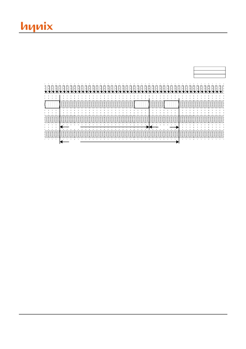
Precharge Mechanisms
Figure 13: shows an example of precharge with the ROWR
packet mechanism. The PRER command must occur a time
t
RAS
after the ACT command, and a time t
RP
before the next
ACT command. This timing will serve as a baseline aginst
which the other precharge mechanisms can be compared.
Figure 14: (top) shows an example of precharge with a RDA
command. A bank is activated with an ROWA packet on the
ROW pins. Then, a series of four dualocts are read with RD
commands in COLC packets on the COL pins. The fourth of
these commands is a RDA, which causes the bank to auto-
matically precharge when the final read has finished. The
timing of this automatic precharge is equivalent to a PRER
command in an ROWR packet on the ROW pins that is
offset a time t
OFFP
from the COLC packet with the RDA
command. The RDA command should be treated as a RD
command in a COLC packet as well as a simultaneous (but
offset) PRER command in an ROWR packet when analyzing
interactions with other packets.
Figure 14: (middle) shows an example of precharge with a
WRA command. As in the RDA example, a bank is acti-
vated with an ROWA packet on the ROW pins. Then, two
dualocts are written with WR commands in COLC packets
on the COL pins. The second of these commands is a WRA,
which causes the bank to automatically precharge when the
final write has been retired. The timing of this automatic
precharge is equivalent to a PRER command in an ROWR
packet on the ROW pins that is offset a time t
OFFP
from the
COLC packet that causes the automatic retire. The WRA
command should be treated as a WR command in a COLC
packet as well as a simultaneous (but offset) PRER
command in an ROWR packet when analyzing interactions
with other packets. Note that the automatic retire is triggered
by a COLC packet a time t
RTR
after the COLC packet with
the WR command unless the second COLC contains a RD
command to the same device. This is described in more
detail in Figure 17:.
Figure 14: (bottom) shows an example of precharge with a
PREX command in an COLX packet. A bank is activated
with an ROWA packet on the ROW pins. Then, a series of
four dualocts are read with RD commands in COLC packets
on the COL pins. The fourth of these COLC packets
includes an COLX packet with a PREC command. This
causes the bank to precharge with timing equivalent to a
PRER command in an ROWR packet on the ROW pins that
is offset a time t
OFFP
from the COLX packet with the PREX
command.
Figure 13: Precharge via PRER Command in ROWR Packet
CTM/CFM
DQA8..0
DQB8..0
COL4
..COL0
ROW2
..ROW0
T
0
T
4
T
8
T
12
T
1
T
5
T
9
T
13
T
2
T
6
T
10
T
14
T
3
T
7
T
11
T
15
T
16
T
20
T
24
T
28
T
17
T
21
T
25
T
29
T
18
T
22
T
26
T
30
T
19
T
23
T
27
T
31
T
32
T
36
T
40
T
44
T
33
T
37
T
41
T
45
T
34
T
38
T
42
T
46
T
35
T
39
T
43
T
47
ACT a0
PRER a5
t
RAS
t
RC
a0 = {Da,Ba,Ra}
a5 = {Da,Ba}
b0 = {Da,Ba,Rb}
t
RP
ACT b0
相关PDF资料 |
PDF描述 |
|---|---|
| HY5R288HC | -|2.5V|8K|40|Direct RDRAM - 288M |
| HY5V16CF | 1Mx16|3.3V|4K|H|SDR SDRAM - 16M |
| HY5V16CF-H | x16 SDRAM |
| HY5V16CF-S | x16 SDRAM |
| HY6116-10 | x8 SRAM |
相关代理商/技术参数 |
参数描述 |
|---|---|
| HY5S2B6DLF-BE | 制造商:HYNIX 制造商全称:Hynix Semiconductor 功能描述:4Banks x 2M x 16bits Synchronous DRAM |
| HY5S2B6DLFP-BE | 制造商:HYNIX 制造商全称:Hynix Semiconductor 功能描述:4Banks x 2M x 16bits Synchronous DRAM |
| HY5S2B6DLFP-SE | 制造商:HYNIX 制造商全称:Hynix Semiconductor 功能描述:4Banks x 2M x 16bits Synchronous DRAM |
| HY5S2B6DLF-SE | 制造商:HYNIX 制造商全称:Hynix Semiconductor 功能描述:4Banks x 2M x 16bits Synchronous DRAM |
| HY5S5B2BLF-6E | 制造商:HYNIX 制造商全称:Hynix Semiconductor 功能描述:256M (8Mx32bit) Mobile SDRAM |
发布紧急采购,3分钟左右您将得到回复。