- 您现在的位置:买卖IC网 > PDF目录67712 > IDT5T2010BBGI (INTEGRATED DEVICE TECHNOLOGY INC) 5T SERIES, PLL BASED CLOCK DRIVER, 10 TRUE OUTPUT(S), 0 INVERTED OUTPUT(S), PBGA144 PDF资料下载
参数资料
| 型号: | IDT5T2010BBGI |
| 厂商: | INTEGRATED DEVICE TECHNOLOGY INC |
| 元件分类: | 时钟及定时 |
| 英文描述: | 5T SERIES, PLL BASED CLOCK DRIVER, 10 TRUE OUTPUT(S), 0 INVERTED OUTPUT(S), PBGA144 |
| 封装: | GREEN, PLASTIC, BGA-144 |
| 文件页数: | 20/24页 |
| 文件大小: | 201K |
| 代理商: | IDT5T2010BBGI |
5
INDUSTRIALTEMPERATURERANGE
IDT5T2010
2.5V ZERO DELAY PLL CLOCK DRIVER TERACLOCK
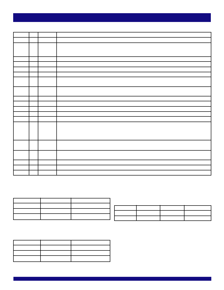
PIN DESCRIPTION, CONTINUED
Symbol
I/O
Type
Description
REF_SEL
I
LVTTL(1)
Reference clock select. When LOW, selects REF0 and
REF0/VREF0. When HIGH, selects REF1 and REF1/VREF1.
nsOE
I
LVTTL(1)
Synchronous output enable. When
nsOEisHIGH,nQ[1:0]aresynchronouslystopped. OMODEselectswhethertheoutputsaregated
LOW/HIGH or tri-stated. When OMODE is HIGH, PE determines the level at which the outputs stop. When PE is LOW/HIGH, the
nQ[1:0] is stopped in a HIGH/LOW state. When OMODE is LOW, the outputs are tri-stated. Set
nsOE LOW for normal operation.
QFB
O
Adjustable(2)
Feedbackclockoutput
QFB
O
Adjustable(2)
Complementary feedback clock output
nQ[1:0]
O
Adjustable(2)
Five banks of two outputs
RxS
I
3-Level(3)
Selects single-ended 2.5V LVTTL (HIGH), 1.8V LVTTL (MID) REF clock input or differential (LOW) REF clock input
TxS
I
3-Level(3)
Sets the drive strength of the output drivers and feedback inputs to be 2.5V LVTTL (HIGH), 1.8V LVTTL (MID) or HSTL/eHSTL (LOW)
compatible. Used in conjuction with VDDQ to set the interface levels.
PE
I
LVTTL(1)
Selectablepositiveornegativeedgecontrol. WhenLOW/HIGHtheoutputsaresynchronizedwiththenegative/positiveedgeofthereference
clock (has internal pull-up).
nF[2:1]
I
LVTTL(1)
Function select inputs for divide-by-2, divide-by-4, zero delay, or invert on each bank (See Control Summary table)
FBF[2:1]
I
LVTTL(1)
Function select inputs for divide-by-2, divide-by-4, zero delay, or invert on the feedback bank (See Control Summary table)
FS
I
LVTTL(1)
Selects appropriate oscillator circuit based on anticipated frequency range. (See VCO Frequency Range Select.)
DS[1:0]
I
3-Level(3)
3-level inputs for feedback input divider selection (See Divide Selection table)
PLL_EN
I
LVTTL(1)
PLL enable/disable control. Set LOW for normal operation. When
PLL_ENisHIGH,thePLLisdisabledandREF[1:0]goestoalloutputs.
PD
I
LVTTL(1)
Power down control. When
PDisLOW,theinputsaredisabledandinternalswitchingisstopped. OMODEselectswhethertheoutputs
are gated LOW/HIGH or tri-stated. When OMODE is HIGH, PE determines the level at which the outputs stop. When PE is LOW/
HIGH, the nQ[1:0] and QFB are stopped in a HIGH/LOW state, while the
QFB is stopped in a LOW/HIGH state. When OMODE is
LOW, the outputs are tri-stated. Set
PD HIGH for normal operation.
LOCK
O
LVTTL
PLL lock indication signal. HIGH indicates lock. LOW indicates that the PLL is not locked and outputs may not be synchronized to the
inputs. The output will be 2.5V LVTTL. (For more information on application specific use of the LOCK pin, please see AN237.)
OMODE
I
LVTTL(1)
Output disable control. Determines the outputs' disable state. Used in conjunction with
nsOEandPD. (SeeOutputEnable/Disableand
Powerdown tables.)
VDDQ
PWR
Power supply for output buffers. When using 2.5V LVTTL, VDDQ should be connected to VDD.
VDD
PWR
Power supply for phase locked loop, lock output, inputs, and other internal circuitry
GND
PWR
Ground
NOTES:
1. Pins listed as LVTTL inputs will accept 2.5V signals under all conditions. If the output is operating at 1.8V or 1.5V, the LVTTL inputs will accept 1.8V LVTTL signals as well.
2. Outputs are user selectable to drive 2.5V, 1.8V LVTTL, eHSTL, or HSTL interface levels when used with the appropriate VDDQ voltage.
3. 3-level inputs are static inputs and must be tied to VDD or GND or left floating. These inputs are not hot-insertable or over voltage tolerant.
NOTE:
1. The level to be set on FS is determined by the nominal operating frequency of the
VCO. The VCO frequency (FNOM) always appears at nQ[1:0] outputs when they are
operated in their undivided modes. The frequency appearing at the REF[1:0] and
REF[1:0] /VREF[1:0] and FB and FB/VREF2 inputs will be FNOM when the QFB and QFB
are undivided and DS[1:0] = MM. The frequency of REF[1:0] and
REF[1:0] /VREF[1:0]
and FB and
FB/VREF2 inputs will be FNOM/2 or FNOM/4 when the part is configured for
frequency multiplication by using a divided QFB and
QFB and setting DS[1:0] = MM.
Using the DS[1:0] inputs allows a different method for frequency multiplication (see
Divide Selection table).
VCO FREQUENCY RANGE SELECT
FS(1)
Min.
Max.
Unit
LOW
50
125
MHz
HIGH
100
250
MHz
NOTE:
1. PE determines the level at which the outputs stop. When PE is LOW/HIGH, the
nQ[1:0] is stopped in a HIGH/LOW state.
OUTPUTENABLE/DISABLE
nsOE
OMODE
Output
L
X
NormalOperation
H
L
Tri-State
H
Gated(1)
NOTE:
1. PE determines the level at which the outputs stop. When PE is LOW/HIGH, the
nQ[1:0] and QFB are stopped in a HIGH/LOW state, while the
QFB is stopped in a
LOW/HIGH state.
POWERDOWN
PD
OMODE
Output
H
X
NormalOperation
L
Tri-State
L
H
Gated(1)
相关PDF资料 |
PDF描述 |
|---|---|
| IDT5T2010BBI8 | 5T SERIES, PLL BASED CLOCK DRIVER, 10 TRUE OUTPUT(S), 0 INVERTED OUTPUT(S), PBGA144 |
| IDT5T9010BBGI | 5T SERIES, PLL BASED CLOCK DRIVER, 5 TRUE OUTPUT(S), 0 INVERTED OUTPUT(S), PBGA144 |
| IDT5T9010BBI | 5T SERIES, PLL BASED CLOCK DRIVER, 5 TRUE OUTPUT(S), 0 INVERTED OUTPUT(S), PBGA144 |
| IDT5T9010BBI8 | 5T SERIES, PLL BASED CLOCK DRIVER, 5 TRUE OUTPUT(S), 0 INVERTED OUTPUT(S), PBGA144 |
| IDT5T905PGGI | 5T SERIES, LOW SKEW CLOCK DRIVER, 5 TRUE OUTPUT(S), 0 INVERTED OUTPUT(S), PDSO28 |
相关代理商/技术参数 |
参数描述 |
|---|---|
| IDT5T2010BBGI8 | 功能描述:IC CLK DVR ZD PLL 2.5V 144-BGA RoHS:是 类别:集成电路 (IC) >> 时钟/计时 - 时钟发生器,PLL,频率合成器 系列:TeraClock™ 标准包装:1,000 系列:- 类型:时钟/频率合成器,扇出分配 PLL:- 输入:- 输出:- 电路数:- 比率 - 输入:输出:- 差分 - 输入:输出:- 频率 - 最大:- 除法器/乘法器:- 电源电压:- 工作温度:- 安装类型:表面贴装 封装/外壳:56-VFQFN 裸露焊盘 供应商设备封装:56-VFQFP-EP(8x8) 包装:带卷 (TR) 其它名称:844S012AKI-01LFT |
| IDT5T2010BBI | 功能描述:IC CLK DVR ZD PLL 2.5V 144-BGA RoHS:否 类别:集成电路 (IC) >> 时钟/计时 - 时钟发生器,PLL,频率合成器 系列:TeraClock™ 标准包装:1,000 系列:- 类型:时钟/频率合成器,扇出分配 PLL:- 输入:- 输出:- 电路数:- 比率 - 输入:输出:- 差分 - 输入:输出:- 频率 - 最大:- 除法器/乘法器:- 电源电压:- 工作温度:- 安装类型:表面贴装 封装/外壳:56-VFQFN 裸露焊盘 供应商设备封装:56-VFQFP-EP(8x8) 包装:带卷 (TR) 其它名称:844S012AKI-01LFT |
| IDT5T2010NLGI | 功能描述:IC CLK DVR ZD PLL 2.5V 68-VFQFPN RoHS:是 类别:集成电路 (IC) >> 时钟/计时 - 时钟发生器,PLL,频率合成器 系列:TeraClock™ 标准包装:1,000 系列:- 类型:时钟/频率合成器,扇出分配 PLL:- 输入:- 输出:- 电路数:- 比率 - 输入:输出:- 差分 - 输入:输出:- 频率 - 最大:- 除法器/乘法器:- 电源电压:- 工作温度:- 安装类型:表面贴装 封装/外壳:56-VFQFN 裸露焊盘 供应商设备封装:56-VFQFP-EP(8x8) 包装:带卷 (TR) 其它名称:844S012AKI-01LFT |
| IDT5T2010NLGI8 | 功能描述:IC CLK DVR ZD PLL 2.5V 68-VFQFPN RoHS:是 类别:集成电路 (IC) >> 时钟/计时 - 时钟发生器,PLL,频率合成器 系列:TeraClock™ 标准包装:1,000 系列:- 类型:时钟/频率合成器,扇出分配 PLL:- 输入:- 输出:- 电路数:- 比率 - 输入:输出:- 差分 - 输入:输出:- 频率 - 最大:- 除法器/乘法器:- 电源电压:- 工作温度:- 安装类型:表面贴装 封装/外壳:56-VFQFN 裸露焊盘 供应商设备封装:56-VFQFP-EP(8x8) 包装:带卷 (TR) 其它名称:844S012AKI-01LFT |
| IDT5T2110BBGI | 功能描述:IC CLK DVR 2.5V PLL DIFF 144BGA RoHS:是 类别:集成电路 (IC) >> 时钟/计时 - 时钟发生器,PLL,频率合成器 系列:TeraClock™ 标准包装:1,000 系列:- 类型:时钟/频率合成器,扇出分配 PLL:- 输入:- 输出:- 电路数:- 比率 - 输入:输出:- 差分 - 输入:输出:- 频率 - 最大:- 除法器/乘法器:- 电源电压:- 工作温度:- 安装类型:表面贴装 封装/外壳:56-VFQFN 裸露焊盘 供应商设备封装:56-VFQFP-EP(8x8) 包装:带卷 (TR) 其它名称:844S012AKI-01LFT |
发布紧急采购,3分钟左右您将得到回复。