- 您现在的位置:买卖IC网 > PDF目录296206 > IDT71V65903S80B (INTEGRATED DEVICE TECHNOLOGY INC) 512K X 18 ZBT SRAM, 8 ns, PBGA119 PDF资料下载
参数资料
| 型号: | IDT71V65903S80B |
| 厂商: | INTEGRATED DEVICE TECHNOLOGY INC |
| 元件分类: | SRAM |
| 英文描述: | 512K X 18 ZBT SRAM, 8 ns, PBGA119 |
| 封装: | 14 X 22 MM, PLASTIC, MS-026AA, BGA-119 |
| 文件页数: | 12/26页 |
| 文件大小: | 972K |
| 代理商: | IDT71V65903S80B |
6.42
2
IDT71V65703, IDT71V65903, 256K x 36, 512K x 18, 3.3V Synchronous ZBT SRAMs with
3.3V I/O, Burst Counter, and Flow-Through Outputs
Commercial and Industrial Temperature Ranges
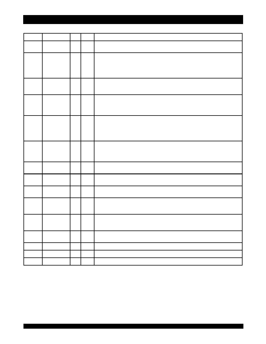
Pin Definitions(1)
NOTE:
1. All synchronous inputs must meet specified setup and hold times with respect to CLK.
Symbol
Pin Function
I/O
Active
Description
A0-A18
Address Inputs
I
N/A
Synchro nous Address inputs. The address register is triggered by a co mbination of the rising edge of
CLK, ADV/
LD low, CEN low, and true chip enables.
ADV/
LD
Advance / Load
I
N/A
ADV/
LD is a synchronous input that is used to load the internal registers with new address and control
when it is sample d low at the rising edge of clock with the chip selected. When ADV/
LD is low with
the chip deselected, any burst in progress is terminated. When ADV/
LD is sampled high then the
inte rnal burst counter is advanced for any burst that was in progress. The external addresses are
ignored when ADV/
LD is sampled high.
R/
W
Read / Write
I
N/A
R/
W signal is a synchronous input that identifies whether the current load cycle initiated is a Read or
Write access to the memory array. The data bus activity for the curre nt cycle takes place one clock
cycle later.
CEN
Clock Enable
I
LOW
Synchronous Clock Enable Input. When
CEN is sampled high, all other synchronous inputs, including
clock are ignored and outputs re main unchanged. The effect of
CEN sampled high on the device
outputs is as if the low to high clock transition did no t occur. For normal operation,
CEN must be
sampled low at rising edge of clock.
BW1-BW4
Individual Byte
Write Enables
I
LOW
Synchronous byte write enables. Each 9-bit byte has its own active low byte write enable. On load
write cycles (When R/
W and ADV/LD are sampled low) the appropriate byte write signal (BW1-BW4)
must be valid. The byte write signal must also be valid on each cycle of a burst write. Byte Write
signals are ignored when R/
W is sampled high. The appropriate byte(s) of data are written into the
device one cycle later.
BW1-BW4 can all be tied low if always doing write to the entire 36-bit word.
CE1, CE2
Chip Enables
I
LOW
Synchronous active low chip enable.
CE1 and CE2 are used with CE2 to enable the IDT71V65703/5903
(
CE1 or CE2 sampled high or CE2 sampled low) and ADV/LD low at the rising edge of clock, initiates
a deselect cycle. The ZBTTM has a one cycle deselect, i.e., the data b us will tri-state one clock cycle
after deselect is initiated.
CE2
Chip Enable
I
HIGH
Synchrono us active high chip enable. CE2 is used with
CE1 and CE2 to enable the chip. CE2 has
inverted po larity but otherwise identical to
CE1 and CE2.
CLK
Clock
I
N/A
This is the clock input to the IDT71V65703/5903. Except for
OE, all timing references for the device are
made with respect to the rising edge of CLK.
I/O0-I/O31
I/OP1-I/OP4
Data Input/Output
I/O
N/A
Data input/output (I/O) pins. The data input path is registered, triggered by the rising edge of CLK. The
data output path is flow-through (no output register).
LBO
Linear Burst
Order
I
LOW
Burst order selection input. When
LBO is high the Interleaved burst sequence is selected. When LBO
is low the Linear burst sequence is selected.
LBO is a static input, and it must not change during
device operation.
OE
Output Enable
I
LOW
Asynchronous output enable.
OE must be low to read data from the 71V65703/5903. When OE is HIGH
the I/O pins are in a high-impedance state.
OE does not need to be actively controlled for read and
write cycles. In normal operation,
OE can be tied low.
ZZ
Sleep Mode
I
HIGH
Asynchro nous sleep mode input. ZZ HIGH will gate the CLK internally and power down the
IDT71V65703/5903 to its lowest power consumption level. Data retention is guaranteed in Sleep Mode.
VDD
Power Supply
N/A
3.3V core power supply.
VDDQ
Power Supply
N/A
3.3V I/O supply.
VSS
Ground
N/A
Ground.
5298 tbl 02
相关PDF资料 |
PDF描述 |
|---|---|
| IDT7210L25PQF | 16-BIT, DSP-MULTIPLIER ACCUMULATOR/SUMMER, PQFP64 |
| IDT7281L25SOI | 512 X 9 OTHER FIFO, 25 ns, PDSO28 |
| 7200L20TDB | 256 X 9 OTHER FIFO, 20 ns, CDIP28 |
| IDT7281L25TPI | 512 X 9 OTHER FIFO, 25 ns, PDIP28 |
| IDT7284L20PAI | 4K X 9 BI-DIRECTIONAL FIFO, 20 ns, PDSO56 |
相关代理商/技术参数 |
参数描述 |
|---|---|
| IDT71V65903S80BG | 功能描述:IC SRAM 9MBIT 80NS 119BGA RoHS:否 类别:集成电路 (IC) >> 存储器 系列:- 标准包装:72 系列:- 格式 - 存储器:RAM 存储器类型:SRAM - 同步 存储容量:9M(256K x 36) 速度:75ns 接口:并联 电源电压:3.135 V ~ 3.465 V 工作温度:-40°C ~ 85°C 封装/外壳:100-LQFP 供应商设备封装:100-TQFP(14x14) 包装:托盘 其它名称:71V67703S75PFGI |
| IDT71V65903S80BG8 | 功能描述:IC SRAM 9MBIT 80NS 119BGA RoHS:否 类别:集成电路 (IC) >> 存储器 系列:- 标准包装:72 系列:- 格式 - 存储器:RAM 存储器类型:SRAM - 同步 存储容量:9M(256K x 36) 速度:75ns 接口:并联 电源电压:3.135 V ~ 3.465 V 工作温度:-40°C ~ 85°C 封装/外壳:100-LQFP 供应商设备封装:100-TQFP(14x14) 包装:托盘 其它名称:71V67703S75PFGI |
| IDT71V65903S80BGI | 功能描述:IC SRAM 9MBIT 80NS 119BGA RoHS:否 类别:集成电路 (IC) >> 存储器 系列:- 标准包装:45 系列:- 格式 - 存储器:RAM 存储器类型:SRAM - 双端口,异步 存储容量:128K(8K x 16) 速度:15ns 接口:并联 电源电压:3 V ~ 3.6 V 工作温度:0°C ~ 70°C 封装/外壳:100-LQFP 供应商设备封装:100-TQFP(14x14) 包装:托盘 其它名称:70V25S15PF |
| IDT71V65903S80BGI8 | 功能描述:IC SRAM 9MBIT 80NS 119BGA RoHS:否 类别:集成电路 (IC) >> 存储器 系列:- 标准包装:72 系列:- 格式 - 存储器:RAM 存储器类型:SRAM - 同步 存储容量:9M(256K x 36) 速度:75ns 接口:并联 电源电压:3.135 V ~ 3.465 V 工作温度:-40°C ~ 85°C 封装/外壳:100-LQFP 供应商设备封装:100-TQFP(14x14) 包装:托盘 其它名称:71V67703S75PFGI |
| IDT71V65903S80BQ | 功能描述:IC SRAM 9MBIT 80NS 165FBGA RoHS:否 类别:集成电路 (IC) >> 存储器 系列:- 标准包装:72 系列:- 格式 - 存储器:RAM 存储器类型:SRAM - 同步 存储容量:9M(256K x 36) 速度:75ns 接口:并联 电源电压:3.135 V ~ 3.465 V 工作温度:-40°C ~ 85°C 封装/外壳:100-LQFP 供应商设备封装:100-TQFP(14x14) 包装:托盘 其它名称:71V67703S75PFGI |
发布紧急采购,3分钟左右您将得到回复。