- 您现在的位置:买卖IC网 > PDF目录175801 > IDT72V265LA10PFI (Integrated Device Technology, Inc.) 3.3 VOLT CMOS SuperSync FIFO 8,192 x 18 16,384 x 18 PDF资料下载
参数资料
| 型号: | IDT72V265LA10PFI |
| 厂商: | Integrated Device Technology, Inc. |
| 英文描述: | 3.3 VOLT CMOS SuperSync FIFO 8,192 x 18 16,384 x 18 |
| 中文描述: | 3.3伏的CMOS SuperSync先进先出8192 × 18 16,384 × 18 |
| 文件页数: | 17/27页 |
| 文件大小: | 439K |
| 代理商: | IDT72V265LA10PFI |
第1页第2页第3页第4页第5页第6页第7页第8页第9页第10页第11页第12页第13页第14页第15页第16页当前第17页第18页第19页第20页第21页第22页第23页第24页第25页第26页第27页
24
IDT72V255LA/72V265LA 3.3 VOLT CMOS SuperSync FIFO
8,192 x 18, 16,384 x 18
COMMERCIAL AND INDUSTRIAL
TEMPERATURE RANGES
NOTES:
1. Use an AND gate in IDT Standard mode, an OR gate in FWFT mode.
2. Do not connect any output control signals directly together.
3. FIFO #1 and FIFO #2 must be the same depth, but may be different word widths.
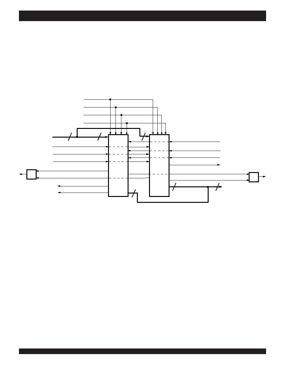
OPTIONAL CONFIGURATIONS
WIDTH EXPANSION CONFIGURATION
Word width may be increased simply by connecting together the
control signals of multiple devices. Status flags can be detected from
any one device. The exceptions are the
EF and FF functions in IDT
Standard mode and the
IR and OR functions in FWFT mode. Because
of variations in skew between RCLK and WCLK, it is possible for
EF/FF
deassertion and
IR/OR assertion to vary by one cycle between FIFOs. In
Figure 19. Block Diagram of 8,192 x 36 and 16,384 x 36 Width Expansion
IDT Standard mode, such problems can be avoided by creating composite
flags, that is, ANDing
EF of every FIFO, and separately ANDing FF of
every FIFO. In FWFT mode, composite flags can be created by ORing
OR of every FIFO, and separately ORing IR of every FIFO.
Figure 23 demonstrates a width expansion using two IDT72V255LA/
72V265LA devices. D0 - D17 from each device form a 36-bit wide input
bus and Q0-Q17 from each device form a 36-bit wide output bus. Any
word width can be attained by adding additional IDT72V255LA/72V265LA
devices.
WRITE CLOCK (WCLK)
m + n
m
n
MASTER RESET (
MRS)
READ CLOCK (RCLK)
DATA OUT
n
m + n
WRITE ENABLE (
WEN)
FULL FLAG/INPUT READY (
FF/IR)
PROGRAMMABLE (
PAF)
PROGRAMMABLE (
PAE)
EMPTY FLAG/OUTPUT READY (
EF/OR) #2
OUTPUT ENABLE (
OE)
READ ENABLE (
REN)
m
LOAD (
LD)
IDT
72V255LA
72V265LA
EMPTY FLAG/OUTPUT READY (
EF/OR) #1
PARTIAL RESET (
PRS)
IDT
72V255LA
72V265LA
4672 drw 22
FULL FLAG/INPUT READY (
FF/IR) #2
HALF-FULL FLAG (
HF)
FIRST WORD FALL THROUGH/
SERIAL INPUT (FWFT/SI)
RETRANSMIT (
RT)
#1
FIFO
#2
GATE
(1)
GATE
(1)
D0 - Dm
DATA IN
Dm+1 - Dn
Q0 - Qm
Qm+1 - Qn
FIFO
#1
相关PDF资料 |
PDF描述 |
|---|---|
| IDT72V265LA10TFI | 3.3 VOLT CMOS SuperSync FIFO 8,192 x 18 16,384 x 18 |
| IDT72V265LA20PFI | Bus buffer/line driver; 3-state - Description: Dual Bus Buffer/Line driver 3-state ; Logic switching levels: CMOS ; Number of pins: 8 ; Output drive capability: +/- 8 mA ; Power dissipation considerations: Low Power or Battery Applications ; Propagation delay: 3.4@5V ns; Voltage: 2.0-5.5 V |
| IDT72V265LA20TFI | 3.3 VOLT CMOS SuperSync FIFO 8,192 x 18 16,384 x 18 |
| IDT72V271LA10TF | 3.3 VOLT CMOS SuperSync FIFO |
| IDT72V271LA15PF | 3.3 VOLT CMOS SuperSync FIFO |
相关代理商/技术参数 |
参数描述 |
|---|---|
| IDT72V265LA10TF | 功能描述:IC FIFO SS 16384X18 10NS 64STQFP RoHS:否 类别:集成电路 (IC) >> 逻辑 - FIFO 系列:72V 标准包装:90 系列:7200 功能:同步 存储容量:288K(16K x 18) 数据速率:100MHz 访问时间:10ns 电源电压:4.5 V ~ 5.5 V 工作温度:0°C ~ 70°C 安装类型:表面贴装 封装/外壳:64-LQFP 供应商设备封装:64-TQFP(14x14) 包装:托盘 其它名称:72271LA10PF |
| IDT72V265LA10TF8 | 功能描述:IC FIFO SS 16384X18 10NS 64STQFP RoHS:否 类别:集成电路 (IC) >> 逻辑 - FIFO 系列:72V 标准包装:90 系列:7200 功能:同步 存储容量:288K(16K x 18) 数据速率:100MHz 访问时间:10ns 电源电压:4.5 V ~ 5.5 V 工作温度:0°C ~ 70°C 安装类型:表面贴装 封装/外壳:64-LQFP 供应商设备封装:64-TQFP(14x14) 包装:托盘 其它名称:72271LA10PF |
| IDT72V265LA10TFG | 功能描述:IC FIFO SS 16384X18 10NS 64STQFP RoHS:是 类别:集成电路 (IC) >> 逻辑 - FIFO 系列:72V 标准包装:90 系列:7200 功能:同步 存储容量:288K(16K x 18) 数据速率:100MHz 访问时间:10ns 电源电压:4.5 V ~ 5.5 V 工作温度:0°C ~ 70°C 安装类型:表面贴装 封装/外壳:64-LQFP 供应商设备封装:64-TQFP(14x14) 包装:托盘 其它名称:72271LA10PF |
| IDT72V265LA10TFG8 | 功能描述:IC FIFO SS 16384X18 10NS 64STQFP RoHS:是 类别:集成电路 (IC) >> 逻辑 - FIFO 系列:72V 标准包装:90 系列:7200 功能:同步 存储容量:288K(16K x 18) 数据速率:100MHz 访问时间:10ns 电源电压:4.5 V ~ 5.5 V 工作温度:0°C ~ 70°C 安装类型:表面贴装 封装/外壳:64-LQFP 供应商设备封装:64-TQFP(14x14) 包装:托盘 其它名称:72271LA10PF |
| IDT72V265LA15PF | 功能描述:IC FIFO SS 16384X18 15NS 64-TQFP RoHS:否 类别:集成电路 (IC) >> 逻辑 - FIFO 系列:72V 标准包装:90 系列:7200 功能:同步 存储容量:288K(16K x 18) 数据速率:100MHz 访问时间:10ns 电源电压:4.5 V ~ 5.5 V 工作温度:0°C ~ 70°C 安装类型:表面贴装 封装/外壳:64-LQFP 供应商设备封装:64-TQFP(14x14) 包装:托盘 其它名称:72271LA10PF |
发布紧急采购,3分钟左右您将得到回复。