- 您现在的位置:买卖IC网 > PDF目录11568 > IDT82V2108BB (IDT, Integrated Device Technology Inc)IC FRAMER T1/J1/E1 8CH 144-BGA PDF资料下载
参数资料
| 型号: | IDT82V2108BB |
| 厂商: | IDT, Integrated Device Technology Inc |
| 文件页数: | 272/292页 |
| 文件大小: | 0K |
| 描述: | IC FRAMER T1/J1/E1 8CH 144-BGA |
| 标准包装: | 10 |
| 控制器类型: | T1/E1/J1 调帧器 |
| 接口: | 并联 |
| 电源电压: | 2.97 V ~ 3.63 V |
| 电流 - 电源: | 160mA |
| 工作温度: | -40°C ~ 85°C |
| 安装类型: | 表面贴装 |
| 封装/外壳: | 144-BGA |
| 供应商设备封装: | 144-PBGA(13x13) |
| 包装: | 托盘 |
| 其它名称: | 82V2108BB |
第1页第2页第3页第4页第5页第6页第7页第8页第9页第10页第11页第12页第13页第14页第15页第16页第17页第18页第19页第20页第21页第22页第23页第24页第25页第26页第27页第28页第29页第30页第31页第32页第33页第34页第35页第36页第37页第38页第39页第40页第41页第42页第43页第44页第45页第46页第47页第48页第49页第50页第51页第52页第53页第54页第55页第56页第57页第58页第59页第60页第61页第62页第63页第64页第65页第66页第67页第68页第69页第70页第71页第72页第73页第74页第75页第76页第77页第78页第79页第80页第81页第82页第83页第84页第85页第86页第87页第88页第89页第90页第91页第92页第93页第94页第95页第96页第97页第98页第99页第100页第101页第102页第103页第104页第105页第106页第107页第108页第109页第110页第111页第112页第113页第114页第115页第116页第117页第118页第119页第120页第121页第122页第123页第124页第125页第126页第127页第128页第129页第130页第131页第132页第133页第134页第135页第136页第137页第138页第139页第140页第141页第142页第143页第144页第145页第146页第147页第148页第149页第150页第151页第152页第153页第154页第155页第156页第157页第158页第159页第160页第161页第162页第163页第164页第165页第166页第167页第168页第169页第170页第171页第172页第173页第174页第175页第176页第177页第178页第179页第180页第181页第182页第183页第184页第185页第186页第187页第188页第189页第190页第191页第192页第193页第194页第195页第196页第197页第198页第199页第200页第201页第202页第203页第204页第205页第206页第207页第208页第209页第210页第211页第212页第213页第214页第215页第216页第217页第218页第219页第220页第221页第222页第223页第224页第225页第226页第227页第228页第229页第230页第231页第232页第233页第234页第235页第236页第237页第238页第239页第240页第241页第242页第243页第244页第245页第246页第247页第248页第249页第250页第251页第252页第253页第254页第255页第256页第257页第258页第259页第260页第261页第262页第263页第264页第265页第266页第267页第268页第269页第270页第271页当前第272页第273页第274页第275页第276页第277页第278页第279页第280页第281页第282页第283页第284页第285页第286页第287页第288页第289页第290页第291页第292页
IDT82V2108
T1 / E1 / J1 OCTAL FRAMER
Functional Description
70
March 5, 2009
3.13.2.1
Transmit Clock Slave Mode
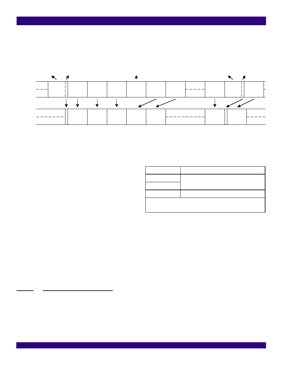
In the Transmit Clock Slave mode, the bit rate on the TSDn pin is
1.544 Mb/s. However, if the system clock rate is 2.048MHz, the data to
be transmitted should be converted into the same rate as the line side,
that is, to work in T1/J1 mode E1 rate. Thus the RATE[1:0] (b3~2, T1/J1-
005H) should be set to ‘01’. The conversion complies as follows: The
last bit of Frame N of the system side is the F-bit of Frame N in the
device. Then one byte of the system side is discarded after the previous
three bytes are converted into the device. This process repeats eight
times and the conversion of one frame is completed. Then the process
goes on (refer to Figure 53).
Figure 53. E1 To T1/J1 Format Conversion
In the Transmit Clock Slave mode, the Transmit Side System Com-
mon Clock B (TSCCKB) is provided by the system side. It is used as a
common timing clock for all eight framers. The speed of TSCCKB can
be 1.544MHz or 2.048MHz. When it is 2.048MHz, TSCCKB can be cho-
sen by the CMS (b5, T1/J1-015H) to be the same as the data (2.048Mb/
S), or double the data (4.096Mb/s). The CMS (b5, T1/J1-015H) of the
eight framers should be set to the same value. If the speed of TSCCKB
is double of the data, there will be two active edges in one bit duration. In
this case, the COFF (b4, T1/J1-015H) determines the active edge to
sample the signal on the TSDn and TSSIGn pins and the active edge to
update the pulse on the TSFSn pin; however, the pulse on TSCFS is
always sampled on its first active edge.
In the Transmit Clock Slave mode, the Transmit Side System Com-
mon Clock A (TSCCKA) is provided by the system side. It is used as one
of the reference clocks for the transmit jitter attenuator DPLL for all eight
framers (refer to Chapter 3.20 Transmit Clock for details).
In the Transmit Clock Slave mode, the Transmit Side System Com-
mon Frame Pulse (TSCFS) is used as a common framing signal to align
data streams for the eight framers. TSCFS is asserted on the request of
each F-bit, the first F-bit of every 12 SFs or every 24 ESFs, as indicated
by the TSCFSP (b1, T1/J1-005H). The valid polarity of TSCFS is config-
ured by the FPINV (b5, T1/J1-005H).
The Transmit Clock Slave Mode includes two sub-modes: Transmit
Clock Slave TSFS Enable Mode and Transmit Clock Slave External Sig-
naling Mode.
3.13.2.1.1
Transmit Clock Slave TSFS Enable Mode
In this mode (refer to Figure 37), the data on the system interface is
clocked by TSCCKB. The active edge of TSCCKB to sample the pulse
on TSCFS and the data on TSDn and TSFSn is determined by the fol-
lowing bits in the registers (refer to Table - 35).
each channel is the first bit to be transmitted.
Besides all the common functions described in the Transmit Clock
Slave mode, the special feature in this mode is that the multi-functional
pin TSFSn/TSSIGn is used as TSFSn to output a framing pulse to indi-
cate every F-bit.
TS0
TS1
TS2
TS3
TS4
TS5
TS6
TS31
TS0
CH1
CH2
CH3
CH4
CH5
CH24
the last bit
F
discarded
the last bit
discarded
F
TS2
CH1
2.048M
bit/s
1.544M
bit/s
Table 35: Active Edge Selection of TSCCKB (in T1/J1 Transmit
Clock Slave TSFS Enable Mode)
the Bit Determining the Active Edge of TSCCKB
TSCFS
TSCCKBFALL (b3, T1/J1-004H)
TSD
TSFS
TSFSRISE (b5, T1/J1-004H)
Note:
The TSCCKBFALL (b3, T1/J1-004H) of the eight framers should be set to the same
value to ensure TSCFS for the eight framers is sampled on the same active edge.
相关PDF资料 |
PDF描述 |
|---|---|
| PIC16LF1936T-I/MV | IC MCU 8BIT 14KB FLASH 28UQFN |
| VI-25K-IX-S | CONVERTER MOD DC/DC 40V 75W |
| IDT82V2108PXG | IC FRAMER T1/J1/E1 8CH 128-PQFP |
| VI-254-IX-S | CONVERTER MOD DC/DC 48V 75W |
| IDT82V2108PX | IC FRAMER T1/J1/E1 8CH 128-PQFP |
相关代理商/技术参数 |
参数描述 |
|---|---|
| IDT82V2108BBG | 功能描述:IC FRAMER T1/J1/E1 8CH 144-BGA RoHS:是 类别:集成电路 (IC) >> 接口 - 控制器 系列:- 标准包装:4,900 系列:- 控制器类型:USB 2.0 控制器 接口:串行 电源电压:3 V ~ 3.6 V 电流 - 电源:135mA 工作温度:0°C ~ 70°C 安装类型:表面贴装 封装/外壳:36-VFQFN 裸露焊盘 供应商设备封装:36-QFN(6x6) 包装:* 其它名称:Q6396337A |
| IDT82V2108PX | 功能描述:IC FRAMER T1/J1/E1 8CH 128-PQFP RoHS:否 类别:集成电路 (IC) >> 接口 - 控制器 系列:- 标准包装:4,900 系列:- 控制器类型:USB 2.0 控制器 接口:串行 电源电压:3 V ~ 3.6 V 电流 - 电源:135mA 工作温度:0°C ~ 70°C 安装类型:表面贴装 封装/外壳:36-VFQFN 裸露焊盘 供应商设备封装:36-QFN(6x6) 包装:* 其它名称:Q6396337A |
| IDT82V2108PX8 | 功能描述:IC FRAMER T1/J1/E1 8CH 128-PQFP RoHS:否 类别:集成电路 (IC) >> 接口 - 控制器 系列:- 标准包装:4,900 系列:- 控制器类型:USB 2.0 控制器 接口:串行 电源电压:3 V ~ 3.6 V 电流 - 电源:135mA 工作温度:0°C ~ 70°C 安装类型:表面贴装 封装/外壳:36-VFQFN 裸露焊盘 供应商设备封装:36-QFN(6x6) 包装:* 其它名称:Q6396337A |
| IDT82V2108PXG | 功能描述:IC FRAMER T1/J1/E1 8CH 128-PQFP RoHS:是 类别:集成电路 (IC) >> 接口 - 控制器 系列:- 标准包装:4,900 系列:- 控制器类型:USB 2.0 控制器 接口:串行 电源电压:3 V ~ 3.6 V 电流 - 电源:135mA 工作温度:0°C ~ 70°C 安装类型:表面贴装 封装/外壳:36-VFQFN 裸露焊盘 供应商设备封装:36-QFN(6x6) 包装:* 其它名称:Q6396337A |
| IDT82V2108PXG8 | 功能描述:IC FRAMER T1/J1/E1 8CH 128-PQFP RoHS:是 类别:集成电路 (IC) >> 接口 - 控制器 系列:- 标准包装:4,900 系列:- 控制器类型:USB 2.0 控制器 接口:串行 电源电压:3 V ~ 3.6 V 电流 - 电源:135mA 工作温度:0°C ~ 70°C 安装类型:表面贴装 封装/外壳:36-VFQFN 裸露焊盘 供应商设备封装:36-QFN(6x6) 包装:* 其它名称:Q6396337A |
发布紧急采购,3分钟左右您将得到回复。