- 您现在的位置:买卖IC网 > PDF目录9580 > IDT82V3010PVG8 (IDT, Integrated Device Technology Inc)IC PLL WAN 51/E1/OC3 DUAL 56SSOP PDF资料下载
参数资料
| 型号: | IDT82V3010PVG8 |
| 厂商: | IDT, Integrated Device Technology Inc |
| 文件页数: | 29/31页 |
| 文件大小: | 0K |
| 描述: | IC PLL WAN 51/E1/OC3 DUAL 56SSOP |
| 标准包装: | 1,000 |
| 类型: | 时钟/频率发生器,多路复用器 |
| PLL: | 是 |
| 主要目的: | 电信 |
| 输入: | 时钟 |
| 输出: | CMOS,LVDS,TTL |
| 电路数: | 1 |
| 比率 - 输入:输出: | 2:12 |
| 差分 - 输入:输出: | 无/是 |
| 频率 - 最大: | 32.768MHz |
| 电源电压: | 3 V ~ 3.6 V |
| 工作温度: | -40°C ~ 85°C |
| 安装类型: | 表面贴装 |
| 封装/外壳: | 56-BSSOP(0.295",7.50mm 宽) |
| 供应商设备封装: | 56-SSOP |
| 包装: | 带卷 (TR) |
| 其它名称: | 82V3010PVG8 |
第1页第2页第3页第4页第5页第6页第7页第8页第9页第10页第11页第12页第13页第14页第15页第16页第17页第18页第19页第20页第21页第22页第23页第24页第25页第26页第27页第28页当前第29页第30页第31页
IDT82V3010
T1/E1/OC3 Telecom Clock Generator with Dual Reference Inputs
Pin Description
7
Feberuary 20, 2009
1
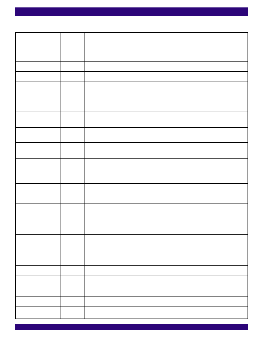
PIN DESCRIPTION
Name
Type
Pin Number
Description
VSS
Power
12, 18, 27
38, 47
Ground.
0 V. All VSS pins should be connected to the ground.
VDDD
Power
13, 19, 26
3.3 V Digital Power Supply.
VDDA
Power
37, 48
3.3 V Analog Power Supply.
OSCi
(CMOS) I
50
Oscillator Master Clock Input.
This pin is connected to a clock source.
Fref0
Fref1
I
5
6
Reference Input 0 and Reference Input 1.
These are two input reference sources (falling edge of 8 kHz, 1.544 MHz and 2.048 MHz or rising edge of 19.44
MHz) used for synchronization. The IN_sel pin determines which one of the two reference inputs to be used. See
Table - 4 for details.
The frequency of the reference inputs can be 8 kHz, 1.544 MHz, 2.048 MHz or 19.44 MHz. These two pins are
internally pulled up to VDDD.
IN_sel
I11
Input Reference Selection.
A logic low at this pin selects Reference Input 0 (Fref0) and a logic high at this pin selects Reference Input 1 (Fref1).
The logic level on this input is gated in by the rising edges of F8o. This Pin is internally pulled down to VSS.
F0_sel0
F0_sel1
I
9
10
Frequency Selection Inputs for Fref0.
These two inputs select one of the four possible frequencies (8 kHz, 1.544 MHz, 2.048 MHz or 19.44 MHz) for the
Reference Input 0 (Fref0). See Table - 2 for details.
F1_sel0
F1_sel1
I
35
34
Frequency Selection Inputs for Fref1.
These two inputs select one of the four possible frequencies (8 kHz, 1.544 MHz, 2.048 MHz or 19.44 MHz) for the
Reference Input 1 (Fref1). These two pins are internally pulled down to Vss. See Table - 3 for details.
MODE_sel0
MODE_sel1
I
1
2
Mode Selection Inputs.
These two inputs determine the operating mode of the IDT82V3010 (Normal, Holdover or Freerun). See Table - 1 for
details.
The logic levels on these two pins are gated in by the rising edges of F8o. These two pins are internally pulled down
to VSS.
RST
I4
Reset Input.
Pulling this pin to logic low for at least 300 ns will reset the IDT82V3010. While the RST pin is low, all framing and
clock outputs are at logic high.
To ensure proper operation, the device must be reset after it is powered up.
TCLR
I3
TIE Control Block Reset.
Pulling this pin to logic low for at least 300 ns will reset the TIE (Maximum Time Interval Error) control block and
result in a realignment of the output phase with the input phase. This pin is internally pulled up to VDDD.
TIE_en
I56
TIE Control Block Enable.
A logic high at this pin enables the TIE control block while a logic low disables it. The logic level on this input is gated
in by the rising edges of F8o. This pin is internally pulled down to Vss.
FLOCK
I45
Fast Lock Mode Enable.
When this pin is set to logic high, the DPLL will quickly lock to the input reference within 500 ms.
LOCK
(CMOS) O
44
Lock Indicator.
This output pin will go high when the DPLL is frequency locked to the input reference.
HOLDOVER
(CMOS) O
52
Holdover Indicator.
This output pin will go high whenever the DPLL enters Holdover mode.
NORMAL
(CMOS) O
46
Normal Indicator.
This output pin will go high whenever the DPLL enters Normal mode.
FREERUN
(CMOS) O
51
Freerun Indicator.
This output pin will go high whenever the DPLL enters Freerun mode.
MON_out0
O
7
Frequency Out-of-range Indicator for Fref0.
A logic high at this pin indicates that Fref0 is off the nominal frequency by more than ±12 ppm.
MON_out1
O
8
Frequency Out-of-range Indicator for Fref1.
A logic high at this pin indicates that Fref1 is off the nominal frequency by more than ±12 ppm.
C19POS
C19NEG
(LVDS) O
21
22
19.44 MHz Clock Output (LVDS Level).
This pair of outputs is used for OC3/STS3 applications.
相关PDF资料 |
PDF描述 |
|---|---|
| D38999/26MF28SN | CONN PLUG 28POS STRAIGHT W/SCKT |
| D38999/26MG16SA | CONN PLUG 16POS STRAIGHT W/SCKT |
| ICS894D115BGI-01 | IC CLK/DATA RECOVERY 20-TSSOP |
| VE-2N0-MX-F2 | CONVERTER MOD DC/DC 5V 75W |
| VI-B1P-MW-F2 | CONVERTER MOD DC/DC 13.8V 100W |
相关代理商/技术参数 |
参数描述 |
|---|---|
| IDT82V3011 | 制造商:IDT 制造商全称:Integrated Device Technology 功能描述:T1/E1/OC3 WAN PLL WITH SINGLE REFERENCE INPUT |
| IDT82V3011PV | 制造商:INT_DEV_TECH 功能描述: |
| IDT82V3011PVG | 功能描述:IC PLL WAN T1/E1/OC3 SGL 56-SSOP RoHS:是 类别:集成电路 (IC) >> 时钟/计时 - 专用 系列:- 标准包装:1,500 系列:- 类型:时钟缓冲器/驱动器 PLL:是 主要目的:- 输入:- 输出:- 电路数:- 比率 - 输入:输出:- 差分 - 输入:输出:- 频率 - 最大:- 电源电压:3.3V 工作温度:0°C ~ 70°C 安装类型:表面贴装 封装/外壳:28-SSOP(0.209",5.30mm 宽) 供应商设备封装:28-SSOP 包装:带卷 (TR) 其它名称:93786AFT |
| IDT82V3011PVG8 | 功能描述:IC PLL WAN T1/E1/OC3 SGL 56-SSOP RoHS:是 类别:集成电路 (IC) >> 时钟/计时 - 专用 系列:- 标准包装:1,500 系列:- 类型:时钟缓冲器/驱动器 PLL:是 主要目的:- 输入:- 输出:- 电路数:- 比率 - 输入:输出:- 差分 - 输入:输出:- 频率 - 最大:- 电源电压:3.3V 工作温度:0°C ~ 70°C 安装类型:表面贴装 封装/外壳:28-SSOP(0.209",5.30mm 宽) 供应商设备封装:28-SSOP 包装:带卷 (TR) 其它名称:93786AFT |
| IDT82V3012 | 制造商:IDT 制造商全称:Integrated Device Technology 功能描述:T1/E1/OC3 WAN PLL WITH DUAL REFERENCE INPUTS |
发布紧急采购,3分钟左右您将得到回复。