- 您现在的位置:买卖IC网 > PDF目录9580 > IDT82V3010PVG8 (IDT, Integrated Device Technology Inc)IC PLL WAN 51/E1/OC3 DUAL 56SSOP PDF资料下载
参数资料
| 型号: | IDT82V3010PVG8 |
| 厂商: | IDT, Integrated Device Technology Inc |
| 文件页数: | 5/31页 |
| 文件大小: | 0K |
| 描述: | IC PLL WAN 51/E1/OC3 DUAL 56SSOP |
| 标准包装: | 1,000 |
| 类型: | 时钟/频率发生器,多路复用器 |
| PLL: | 是 |
| 主要目的: | 电信 |
| 输入: | 时钟 |
| 输出: | CMOS,LVDS,TTL |
| 电路数: | 1 |
| 比率 - 输入:输出: | 2:12 |
| 差分 - 输入:输出: | 无/是 |
| 频率 - 最大: | 32.768MHz |
| 电源电压: | 3 V ~ 3.6 V |
| 工作温度: | -40°C ~ 85°C |
| 安装类型: | 表面贴装 |
| 封装/外壳: | 56-BSSOP(0.295",7.50mm 宽) |
| 供应商设备封装: | 56-SSOP |
| 包装: | 带卷 (TR) |
| 其它名称: | 82V3010PVG8 |
第1页第2页第3页第4页当前第5页第6页第7页第8页第9页第10页第11页第12页第13页第14页第15页第16页第17页第18页第19页第20页第21页第22页第23页第24页第25页第26页第27页第28页第29页第30页第31页
IDT82V3010
T1/E1/OC3 Telecom Clock Generator with Dual Reference Inputs
Functional Description
13
Feberuary 20, 2009
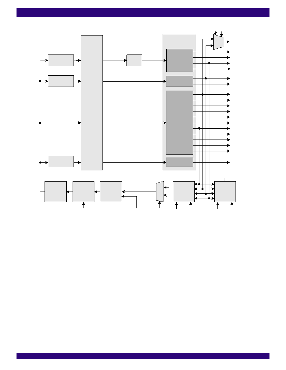
Figure - 7 DPLL Block Diagram
In the Normal mode, the Limiter receives the error signal from the
Phase Detector, limits the phase slope within 5 ns per 125 s and sends
the limited signal to the Loop Filter.
In the Fast Lock mode, the Limiter is disabled, and the DPLL locks to
the input reference within 500 ms, which is much shorter than that in the
Normal mode.
2.7.3
LOOP FILTER
The Loop Filter ensures that the jitter transfer meets the ETS 300
011 and AT&T TR62411 requirements. It works similarly to a first order
low pass filter with 2.1 Hz cutoff frequency for the four valid input
frequencies (8 kHz, 1.544 MHz, 2.048 MHz or 19.44 MHz).
The output of the Loop Filter goes to the Digital Control Oscillator
directly or through the Fraction blocks, in which E1, T1, C6 and C19
signals are generated.
2.7.4
FRACTION BLOCK
By applying some algorithms to the incoming E1 signal, the
Fraction_C19, Fraction_C6 and Fraction_T1 blocks generate C19, C6
and T1 signals respectively.
2.7.5
DIGITAL CONTROL OSCILLATOR (DCO)
In the Normal mode, the DCO receives four limited and filtered
signals from Loop Filter or Fraction blocks. Based on the values of the
received signals, the DCO generates four digital outputs: 19.44 MHz,
25.248 MHz, 32.768 MHz and 24.704 MHz for C19, C6, E1 and T1
dividers respectively.
In the Holdover mode, the DCO is running at the same frequency as
that generated by storage techniques.
In the Freerun mode, the DCO is running at the same frequency as
that of the master clock.
2.7.6
LOCK INDICATOR
If the output frequency of the DPLL is identical to the input frequency,
and the input phase offset is small enough so that no slope limiting is
exhibited, the LOCK pin will be set high.
2.7.7
OUTPUT INTERFACE
The Output Interface uses three output signals from the DCO to
generate totally 9 types of clock signals and 7 types of framing signals
All these output signals are synchronous to F8o.
Digit
al
Co
nt
ro
lOs
cilla
tor
C32o
C16o
C8o
C4o
C2o
C3o
C6o
F0o
F8o
RSP
TSP
F16o
C1.5o
F32o
Output Interface
T1_Divider
E1_Divider
C6_Divider
Frequency
Selection
Circuit 1
Phase
Detector
Virtual Reference
Fraction_C6
Fraction_T1
24.704 MHz
32.768 MHz
25.248 MHz
Feedback Signal
Limiter
FLOCK
F1_sel1 F1_sel0
C19_Divider
155.52 MHz
F19o
C19o
APLL
19.44 MHz
Fraction_C19
C19NEG
C19POS
IN_sel
F0_sel1 F0_sel0
Frequency
Selection
Circuit 0
C2/C1.5
Loop Filter
Fx_sel1 Fx_sel0 (x = 0 or 1)
相关PDF资料 |
PDF描述 |
|---|---|
| D38999/26MF28SN | CONN PLUG 28POS STRAIGHT W/SCKT |
| D38999/26MG16SA | CONN PLUG 16POS STRAIGHT W/SCKT |
| ICS894D115BGI-01 | IC CLK/DATA RECOVERY 20-TSSOP |
| VE-2N0-MX-F2 | CONVERTER MOD DC/DC 5V 75W |
| VI-B1P-MW-F2 | CONVERTER MOD DC/DC 13.8V 100W |
相关代理商/技术参数 |
参数描述 |
|---|---|
| IDT82V3011 | 制造商:IDT 制造商全称:Integrated Device Technology 功能描述:T1/E1/OC3 WAN PLL WITH SINGLE REFERENCE INPUT |
| IDT82V3011PV | 制造商:INT_DEV_TECH 功能描述: |
| IDT82V3011PVG | 功能描述:IC PLL WAN T1/E1/OC3 SGL 56-SSOP RoHS:是 类别:集成电路 (IC) >> 时钟/计时 - 专用 系列:- 标准包装:1,500 系列:- 类型:时钟缓冲器/驱动器 PLL:是 主要目的:- 输入:- 输出:- 电路数:- 比率 - 输入:输出:- 差分 - 输入:输出:- 频率 - 最大:- 电源电压:3.3V 工作温度:0°C ~ 70°C 安装类型:表面贴装 封装/外壳:28-SSOP(0.209",5.30mm 宽) 供应商设备封装:28-SSOP 包装:带卷 (TR) 其它名称:93786AFT |
| IDT82V3011PVG8 | 功能描述:IC PLL WAN T1/E1/OC3 SGL 56-SSOP RoHS:是 类别:集成电路 (IC) >> 时钟/计时 - 专用 系列:- 标准包装:1,500 系列:- 类型:时钟缓冲器/驱动器 PLL:是 主要目的:- 输入:- 输出:- 电路数:- 比率 - 输入:输出:- 差分 - 输入:输出:- 频率 - 最大:- 电源电压:3.3V 工作温度:0°C ~ 70°C 安装类型:表面贴装 封装/外壳:28-SSOP(0.209",5.30mm 宽) 供应商设备封装:28-SSOP 包装:带卷 (TR) 其它名称:93786AFT |
| IDT82V3012 | 制造商:IDT 制造商全称:Integrated Device Technology 功能描述:T1/E1/OC3 WAN PLL WITH DUAL REFERENCE INPUTS |
发布紧急采购,3分钟左右您将得到回复。