- 您现在的位置:买卖IC网 > PDF目录9580 > IDT82V3010PVG8 (IDT, Integrated Device Technology Inc)IC PLL WAN 51/E1/OC3 DUAL 56SSOP PDF资料下载
参数资料
| 型号: | IDT82V3010PVG8 |
| 厂商: | IDT, Integrated Device Technology Inc |
| 文件页数: | 31/31页 |
| 文件大小: | 0K |
| 描述: | IC PLL WAN 51/E1/OC3 DUAL 56SSOP |
| 标准包装: | 1,000 |
| 类型: | 时钟/频率发生器,多路复用器 |
| PLL: | 是 |
| 主要目的: | 电信 |
| 输入: | 时钟 |
| 输出: | CMOS,LVDS,TTL |
| 电路数: | 1 |
| 比率 - 输入:输出: | 2:12 |
| 差分 - 输入:输出: | 无/是 |
| 频率 - 最大: | 32.768MHz |
| 电源电压: | 3 V ~ 3.6 V |
| 工作温度: | -40°C ~ 85°C |
| 安装类型: | 表面贴装 |
| 封装/外壳: | 56-BSSOP(0.295",7.50mm 宽) |
| 供应商设备封装: | 56-SSOP |
| 包装: | 带卷 (TR) |
| 其它名称: | 82V3010PVG8 |
第1页第2页第3页第4页第5页第6页第7页第8页第9页第10页第11页第12页第13页第14页第15页第16页第17页第18页第19页第20页第21页第22页第23页第24页第25页第26页第27页第28页第29页第30页当前第31页
IDT82V3010
T1/E1/OC3 Telecom Clock Generator with Dual Reference Inputs
Functional Description
9
Feberuary 20, 2009
2
FUNCTIONAL DESCRIPTION
The IDT82V3010 is a T1/E1/OC3 telecom clock generator with dual
reference inputs, providing timing (clock) and synchronization (framing)
signals to interface circuits for multitrunk T1/E1 and STS3/OC3 links.
The details are described in the following sections.
2.1
STATE CONTROL CIRCUIT
The State Control Circuit is an important part in the IDT82V3010. It is
used to control the TIE block and the DPLL block as shown in Figure - 2.
The control is based on the result of Invalid Input Signal Detection and
the logic levels on the MODE_sel0, MODE_sel1, IN_sel and TIE_en
pins.
The IDT82V3010 can be operated in three different modes: Normal,
Holdover and Freerun. The operating mode is selected by the
MODE_sel1 and MODE_sel0 pins, as shown in Table - 1.
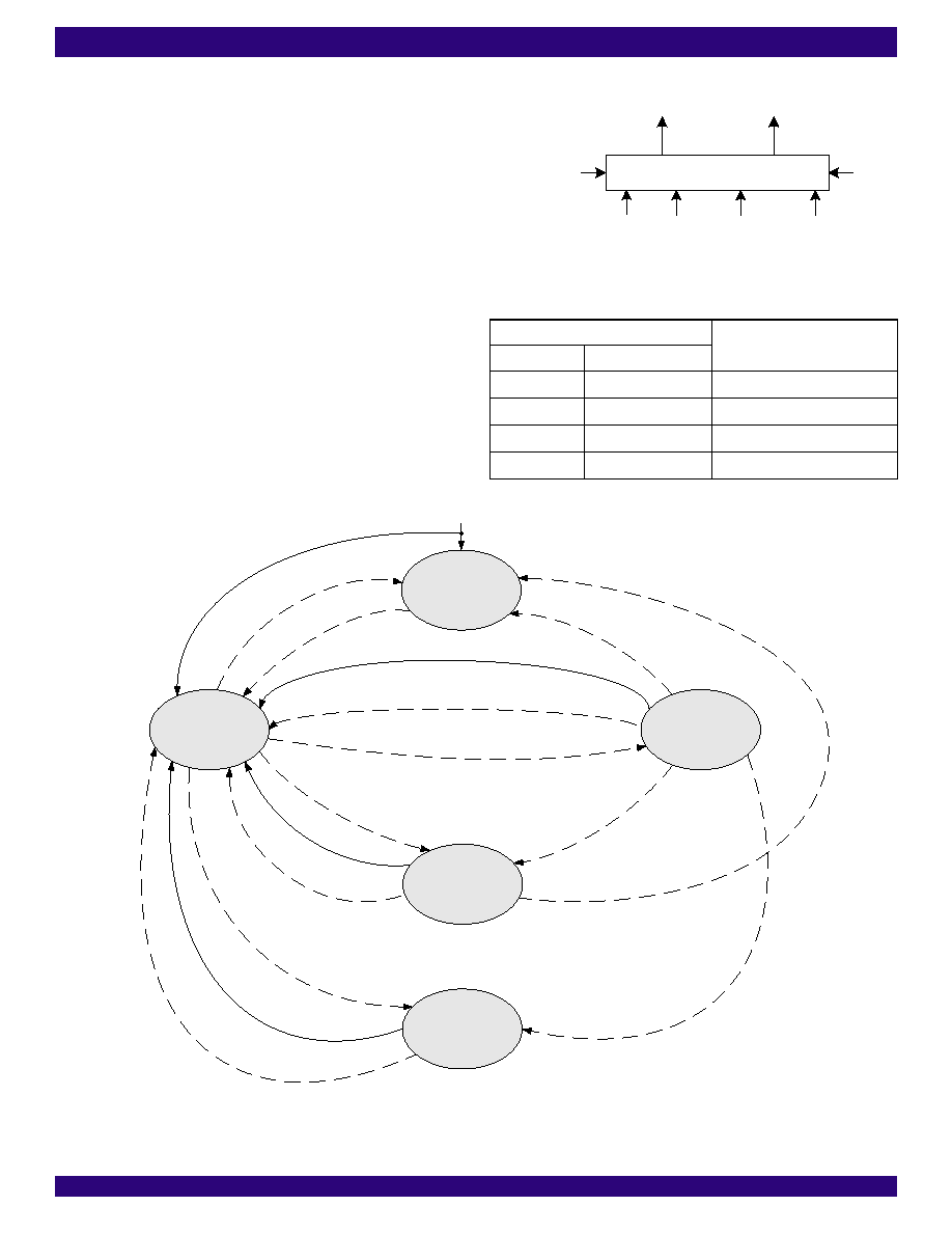
Figure - 3 shows the state control diagram. All state changes occur
synchronously on the rising edge of F8o. Three operating modes,
Normal (S1), Holdover (S3) and Freerun (S0) can be switched from one
to another by changing the logic levels on the MODE_sel0 and
MODE_sel1 pins.
Figure - 2 State Control Circuit
Figure - 3 State Control Diagram
Table - 1 Operating Modes Selection
Mode Selection Pins
Operating Mode
MODE_sel1
MODE_sel0
00
Normal
0
1
Holdover
1
0
Freerun
11
Reserved
State Control Circuit
MODE_sel1 MODE_sel0
TIE_en
Output of the
Invalid Input
Signal Detection
F8o
TIE Block
Enable/Disable
DPLL Block
Mode Control
IN_sel
S1
Normal
Mode_sel1 = 0
Mode_sel0 = 0
S3
Holdover
Mode_sel1 = 0
Mode_sel0 = 1
S0
Freerun
Mode_sel1 = 1
Mode_sel0 = 0
(Invalid Input Reference Signal)
(Valid Input Reference Signal)
Aut
o T
IE D
isab
le
Aut
o T
IE D
isab
le
TIE Enable (TIE_en = H)
AutoT
IE Dis
able
AutoTIE
Disable
Au
to
TIE
Dis
ab
le
TIE
Disa
ble
(TIE
_en
= L)
AutoT
IE Dis
able
TIE E
nable
(TIE_
en =
H)
Reset *
S4
Short Time Holdover
Mode_sel1 = 0
Mode_sel0 = 0
IN_
sel
Tra
nsie
nt
Auto
TIE
Dis
able
No IN
_sel T
ransie
nt
TIE E
nable
(TIE_
en =
H)
No
IN
_s
el
Tra
ns
ien
t
TIE
D
isa
ble
(T
IE
_e
n
=
L)
IN_s
el Tra
nsien
t
Auto
TIE D
isable
S2
Auto - Holdover
Mode_sel1 = 0
Mode_sel0 = 0
* Note: After reset, the Mode_sel1 and Mode_sel0 should be initially set to '10' or '00'.
Auto TIE Disable
(Valid Input Reference Signal)
TIE Disable (TIE_en = L)
相关PDF资料 |
PDF描述 |
|---|---|
| D38999/26MF28SN | CONN PLUG 28POS STRAIGHT W/SCKT |
| D38999/26MG16SA | CONN PLUG 16POS STRAIGHT W/SCKT |
| ICS894D115BGI-01 | IC CLK/DATA RECOVERY 20-TSSOP |
| VE-2N0-MX-F2 | CONVERTER MOD DC/DC 5V 75W |
| VI-B1P-MW-F2 | CONVERTER MOD DC/DC 13.8V 100W |
相关代理商/技术参数 |
参数描述 |
|---|---|
| IDT82V3011 | 制造商:IDT 制造商全称:Integrated Device Technology 功能描述:T1/E1/OC3 WAN PLL WITH SINGLE REFERENCE INPUT |
| IDT82V3011PV | 制造商:INT_DEV_TECH 功能描述: |
| IDT82V3011PVG | 功能描述:IC PLL WAN T1/E1/OC3 SGL 56-SSOP RoHS:是 类别:集成电路 (IC) >> 时钟/计时 - 专用 系列:- 标准包装:1,500 系列:- 类型:时钟缓冲器/驱动器 PLL:是 主要目的:- 输入:- 输出:- 电路数:- 比率 - 输入:输出:- 差分 - 输入:输出:- 频率 - 最大:- 电源电压:3.3V 工作温度:0°C ~ 70°C 安装类型:表面贴装 封装/外壳:28-SSOP(0.209",5.30mm 宽) 供应商设备封装:28-SSOP 包装:带卷 (TR) 其它名称:93786AFT |
| IDT82V3011PVG8 | 功能描述:IC PLL WAN T1/E1/OC3 SGL 56-SSOP RoHS:是 类别:集成电路 (IC) >> 时钟/计时 - 专用 系列:- 标准包装:1,500 系列:- 类型:时钟缓冲器/驱动器 PLL:是 主要目的:- 输入:- 输出:- 电路数:- 比率 - 输入:输出:- 差分 - 输入:输出:- 频率 - 最大:- 电源电压:3.3V 工作温度:0°C ~ 70°C 安装类型:表面贴装 封装/外壳:28-SSOP(0.209",5.30mm 宽) 供应商设备封装:28-SSOP 包装:带卷 (TR) 其它名称:93786AFT |
| IDT82V3012 | 制造商:IDT 制造商全称:Integrated Device Technology 功能描述:T1/E1/OC3 WAN PLL WITH DUAL REFERENCE INPUTS |
发布紧急采购,3分钟左右您将得到回复。