- 您现在的位置:买卖IC网 > PDF目录9580 > IDT82V3010PVG8 (IDT, Integrated Device Technology Inc)IC PLL WAN 51/E1/OC3 DUAL 56SSOP PDF资料下载
参数资料
| 型号: | IDT82V3010PVG8 |
| 厂商: | IDT, Integrated Device Technology Inc |
| 文件页数: | 6/31页 |
| 文件大小: | 0K |
| 描述: | IC PLL WAN 51/E1/OC3 DUAL 56SSOP |
| 标准包装: | 1,000 |
| 类型: | 时钟/频率发生器,多路复用器 |
| PLL: | 是 |
| 主要目的: | 电信 |
| 输入: | 时钟 |
| 输出: | CMOS,LVDS,TTL |
| 电路数: | 1 |
| 比率 - 输入:输出: | 2:12 |
| 差分 - 输入:输出: | 无/是 |
| 频率 - 最大: | 32.768MHz |
| 电源电压: | 3 V ~ 3.6 V |
| 工作温度: | -40°C ~ 85°C |
| 安装类型: | 表面贴装 |
| 封装/外壳: | 56-BSSOP(0.295",7.50mm 宽) |
| 供应商设备封装: | 56-SSOP |
| 包装: | 带卷 (TR) |
| 其它名称: | 82V3010PVG8 |
第1页第2页第3页第4页第5页当前第6页第7页第8页第9页第10页第11页第12页第13页第14页第15页第16页第17页第18页第19页第20页第21页第22页第23页第24页第25页第26页第27页第28页第29页第30页第31页
IDT82V3010
T1/E1/OC3 Telecom Clock Generator with Dual Reference Inputs
Functional Description
14
Feberuary 20, 2009
The 32.768 MHz signal is used by the E1_divider to generate five
types of clock signals (C2o, C4o, C8o, C16o and C32o) with nominal
50% duty cycle and six types of framing signals (F0o, F8o, F16o, F32o,
RSP and TSP).
The 24.704 MHz signal is used by the T1_divider to generate two
types of T1 signals (C1.5o and C3o) with nominal 50% duty cycle.
The 25.248 MHz signal is used by the C6_divider to generate a C6o
signal with nominal 50% duty cycle.
The 19.44 MHz signal is sent to an APLL, which outputs a 155.52
MHz signal. The 155.52 MHz signal is used by the C19_divider to
generate 19.44 MHz clock signals (C19o, C19POS and C19NEG) with
nominal 50% duty cycle and a framing signal F19o.
Additionally, the IDT82V3010 provides an output clock (C2/C1.5)
with the frequency controlled by the frequency selection pins Fx_sel0
and Fx_sel1 (see Table - 5 for details). If the selected reference input
(Fref0 or Fref1) is 8 kHz, 2.048 MHz or 19.44 MHz, the C2/C1.5 pin will
output a 2.048 MHz clock signal. If the selected reference input (Fref0 or
Fref1) is 1.544 MHz, the C2/C1.5 pin will output a 1.544 MHz clock
signal. The electrical and timing characteristics of this output (2.048
MHz or 1.544 MHz) is the same as that of C2o or C1.5o.
2.8
OSC
The IDT82V3010 can use a clock as the master timing source. In the
Freerun mode, the frequency tolerance of the clock outputs is identical
to that of the source at the OSCi pin. For applications not requiring an
accurate Freerun mode, the tolerance of the master timing source may
be ±100 ppm. For applications requiring an accurate Freerun mode,
such as AT&T TR62411, the tolerance of the master timing source must
be no greater than ±32 ppm.
The desired capture range should be taken into consideration when
determining the accuracy of the master timing source. The sum of the
accuracy of the master timing source and the capture range of the
IDT82V3010 will always equal 230 ppm. For example, if the master
timing source is 100 ppm, the capture range will be 130 ppm.
2.8.1
CLOCK OSCILLATOR
When selecting a Clock Oscillator, numerous parameters must be
considered. This includes absolute frequency, frequency change over
temperature, output rise and fall times, output levels and duty cycle.
For applications requiring ±32 ppm clock accuracy, the following
clock oscillator module may be used.
FOX F7C-2E3-20.0 MHz
Frequency:
20.0 MHz
Tolerance:
25 ppm 0
°C to 70°C
Rise & Fall Time:10 ns (0.33 V, 2.97 V, 15 pF)
Duty Cycle:
40% to 60%
The output clock should be connected directly (not AC coupled) to
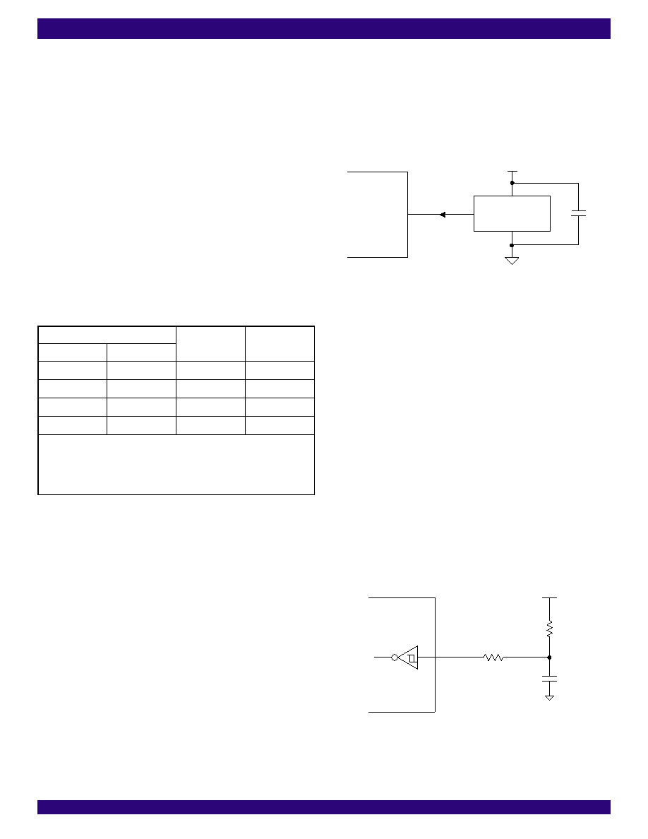
the OSCi input of the IDT82V3010, as shown in Figure - 8.
Figure - 8 Clock Oscillator Circuit
2.9
JTAG
The IDT82V3010 supports IEEE 1149.1 JTAG Scan.
2.10
RESET, LOCK AND TIE APPLICATION
A simple power-up reset circuit is shown as Figure - 9. The logic low
reset pulse is about 50 s.
The resistor Rp is used for protection only and limits current into the
RST pin during power down. The logic low reset pulse width is not
critical but should be greater than 300 ns.
When the DPLL operates in Normal mode after power-up or reset,
the lock pin may indicate frequency lock before the output phase is
synchronized with the input. The phase lock requires 30 seconds (at
most) after frequency lock.
If users want to switch the input reference, it is highly recommended
to do the switch after phase lock, with TIE control block enabled.
After TIE control block is cleared, the DPLL requires some time for
the phase relationship to stabilize. In general, the phase lock requires 30
seconds (at most) after frequency lock.
Figure - 9 Power-Up Reset Circuit
Table - 5 C2/C1.5 Output Frequency Control
Frequency Selection Pins
Frefx Input
Frequency
C2/C1.5 Output
Frequency
Fx_sel1
Fx_sel0
0
19.44 MHz
2.048 MHz
0
1
8 kHz
2.048 MHz
1
0
1.544 MHz
1
2.048 MHz
Note: ‘x’ can be 0 or 1, as selected by IN_sel pin.
IN_sel = 0: x = 0, Fref0 is the selected reference input. The frequency of Fref0
is determined by F0_sel0 and F0_sel1 pins.
IN_sel = 1: x = 1, Fref1 is the selected reference input. The frequency of Fref1
is determined by F1_sel0 and F1_sel1 pins.
+3.3 V
20 MHz OUT
GND
+3.3 V
OSCi
IDT82V3010
0.1
F
3.3 V
R
10 k
Rp
1 k
C
1
F
RST
IDT82V3010
相关PDF资料 |
PDF描述 |
|---|---|
| D38999/26MF28SN | CONN PLUG 28POS STRAIGHT W/SCKT |
| D38999/26MG16SA | CONN PLUG 16POS STRAIGHT W/SCKT |
| ICS894D115BGI-01 | IC CLK/DATA RECOVERY 20-TSSOP |
| VE-2N0-MX-F2 | CONVERTER MOD DC/DC 5V 75W |
| VI-B1P-MW-F2 | CONVERTER MOD DC/DC 13.8V 100W |
相关代理商/技术参数 |
参数描述 |
|---|---|
| IDT82V3011 | 制造商:IDT 制造商全称:Integrated Device Technology 功能描述:T1/E1/OC3 WAN PLL WITH SINGLE REFERENCE INPUT |
| IDT82V3011PV | 制造商:INT_DEV_TECH 功能描述: |
| IDT82V3011PVG | 功能描述:IC PLL WAN T1/E1/OC3 SGL 56-SSOP RoHS:是 类别:集成电路 (IC) >> 时钟/计时 - 专用 系列:- 标准包装:1,500 系列:- 类型:时钟缓冲器/驱动器 PLL:是 主要目的:- 输入:- 输出:- 电路数:- 比率 - 输入:输出:- 差分 - 输入:输出:- 频率 - 最大:- 电源电压:3.3V 工作温度:0°C ~ 70°C 安装类型:表面贴装 封装/外壳:28-SSOP(0.209",5.30mm 宽) 供应商设备封装:28-SSOP 包装:带卷 (TR) 其它名称:93786AFT |
| IDT82V3011PVG8 | 功能描述:IC PLL WAN T1/E1/OC3 SGL 56-SSOP RoHS:是 类别:集成电路 (IC) >> 时钟/计时 - 专用 系列:- 标准包装:1,500 系列:- 类型:时钟缓冲器/驱动器 PLL:是 主要目的:- 输入:- 输出:- 电路数:- 比率 - 输入:输出:- 差分 - 输入:输出:- 频率 - 最大:- 电源电压:3.3V 工作温度:0°C ~ 70°C 安装类型:表面贴装 封装/外壳:28-SSOP(0.209",5.30mm 宽) 供应商设备封装:28-SSOP 包装:带卷 (TR) 其它名称:93786AFT |
| IDT82V3012 | 制造商:IDT 制造商全称:Integrated Device Technology 功能描述:T1/E1/OC3 WAN PLL WITH DUAL REFERENCE INPUTS |
发布紧急采购,3分钟左右您将得到回复。