- 您现在的位置:买卖IC网 > PDF目录2000 > IDT82V3358EDG (IDT, Integrated Device Technology Inc)IC PLL WAN SYNC ETHERNET 64TQFP PDF资料下载
参数资料
| 型号: | IDT82V3358EDG |
| 厂商: | IDT, Integrated Device Technology Inc |
| 文件页数: | 47/139页 |
| 文件大小: | 0K |
| 描述: | IC PLL WAN SYNC ETHERNET 64TQFP |
| 标准包装: | 160 |
| 类型: | 时钟/频率发生器,多路复用器 |
| PLL: | 是 |
| 主要目的: | 以太网,SONET/SDH,Stratum |
| 输入: | CMOS,LVDS,PECL |
| 输出: | CMOS,LVDS,PECL |
| 电路数: | 1 |
| 比率 - 输入:输出: | 2:4 |
| 差分 - 输入:输出: | 是/是 |
| 频率 - 最大: | 622.08MHz |
| 电源电压: | 3 V ~ 3.6 V |
| 工作温度: | -40°C ~ 85°C |
| 安装类型: | 表面贴装 |
| 封装/外壳: | 64-TQFP 裸露焊盘 |
| 供应商设备封装: | 64-TQFP-EP(10x10) |
| 包装: | 托盘 |
第1页第2页第3页第4页第5页第6页第7页第8页第9页第10页第11页第12页第13页第14页第15页第16页第17页第18页第19页第20页第21页第22页第23页第24页第25页第26页第27页第28页第29页第30页第31页第32页第33页第34页第35页第36页第37页第38页第39页第40页第41页第42页第43页第44页第45页第46页当前第47页第48页第49页第50页第51页第52页第53页第54页第55页第56页第57页第58页第59页第60页第61页第62页第63页第64页第65页第66页第67页第68页第69页第70页第71页第72页第73页第74页第75页第76页第77页第78页第79页第80页第81页第82页第83页第84页第85页第86页第87页第88页第89页第90页第91页第92页第93页第94页第95页第96页第97页第98页第99页第100页第101页第102页第103页第104页第105页第106页第107页第108页第109页第110页第111页第112页第113页第114页第115页第116页第117页第118页第119页第120页第121页第122页第123页第124页第125页第126页第127页第128页第129页第130页第131页第132页第133页第134页第135页第136页第137页第138页第139页
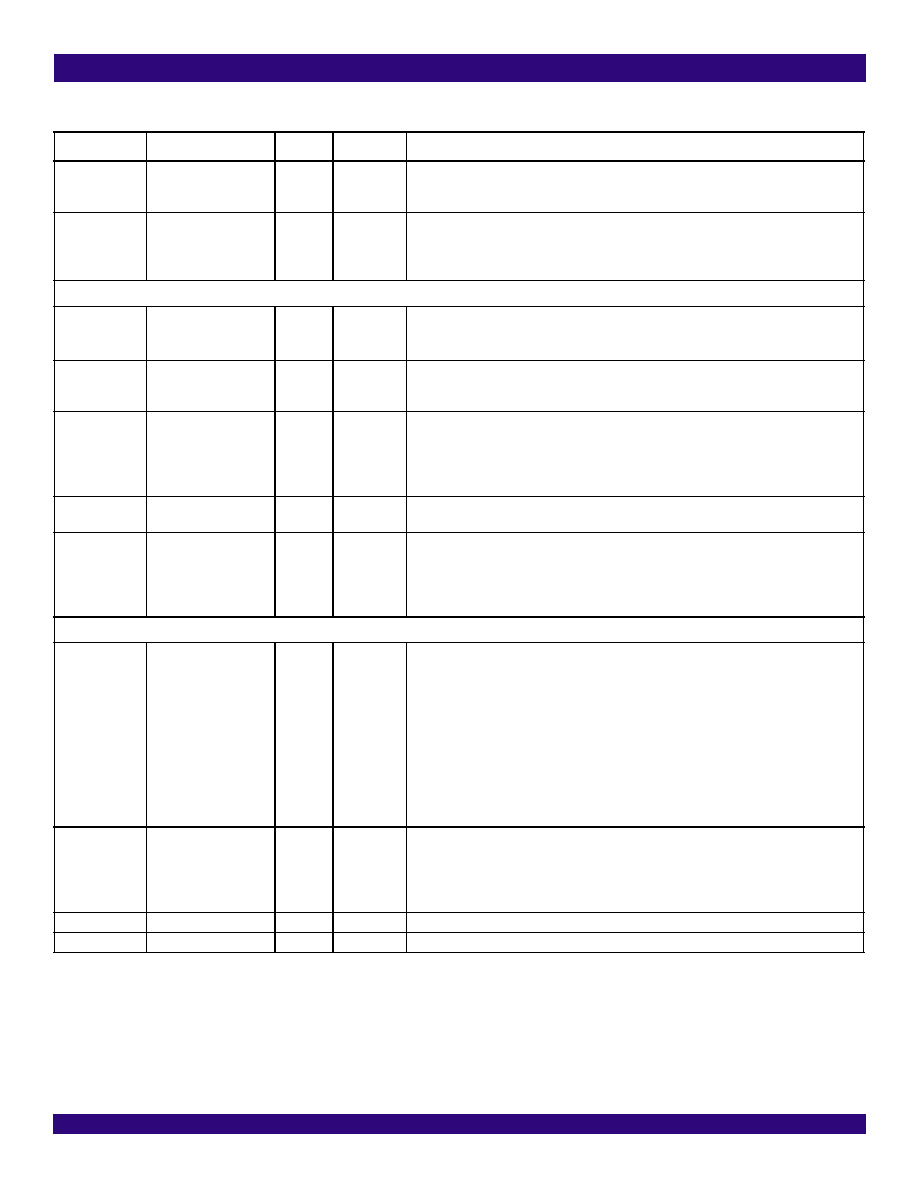
IDT82V3358
SYNCHRONOUS ETHERNET WAN PLL
Pin Description
15
May 19, 2009
SDO
52
I/O
pull-down
CMOS
SDO: Serial Data Output
In Serial mode, this pin is used as the serial data output. Data on this pin is serially clocked
out of the device on the active edge of SCLK.
SCLK
47
I
pull-down
CMOS
SCLK: Shift Clock
In Serial mode, a shift clock is input on this pin.
Data on SDI is sampled by the device on the rising edge of SCLK. Data on SDO is updated
on the active edge of SCLK. The active edge is determined by the CLKE.
JTAG (per IEEE 1149.1)
TRST
37
I
pull-down
CMOS
TRST: JTAG Test Reset (Active Low)
A low signal on this pin resets the JTAG test port.
This pin should be connected to ground when JTAG is not used.
TMS
41
I
pull-up
CMOS
TMS: JTAG Test Mode Select
The signal on this pin controls the JTAG test performance and is sampled on the rising edge
of TCK.
TCK
49
I
pull-down
CMOS
TCK: JTAG Test Clock
The clock for the JTAG test is input on this pin. TDI and TMS are sampled on the rising edge
of TCK and TDO is updated on the falling edge of TCK.
If TCK is idle at a low level, all stored-state devices contained in the test logic will indefinitely
retain their state.
TDI
51
I
pull-up
CMOS
TDI: JTAG Test Data Input
The test data is input on this pin. It is clocked into the device on the rising edge of TCK.
TDO
50
O
CMOS
TDO: JTAG Test Data Output
The test data is output on this pin. It is clocked out of the device on the falling edge of TCK.
TDO pin outputs a high impedance signal except during the process of data scanning.
This pin can indicate the interrupt of T0 selected input clock fail, as determined by the
LOS_FLAG_ON_TDO bit (b6, 0BH). Refer to Chapter 3.8.1 Input Clock Validity for details.
Power & Ground
VDDD1
VDDD2
VDDD3
VDDD4
VDDD5
VDDD6
8
12
9
32
36, 38, 39, 45, 46
54
Power
-
VDDDn: 3.3 V Digital Power Supply
Each VDDDn should be paralleled with ground through a 0.1 F capacitor.
VDDA1
VDDA2
VDDA3
4
14
57
Power
-
VDDAn: 3.3 V Analog Power Supply
Each VDDAn should be paralleled with ground through a 0.1 F capacitor.
VDD_DIFF
22
Power
-
VDD_DIFF: 3.3 V Power Supply for OUT
GND_DIFF
21
Ground
-
GND_DIFF: Ground for OUT1
Table 1: Pin Description (Continued)
Name
Pin No.
I/O
Type
Description 1
相关PDF资料 |
PDF描述 |
|---|---|
| IDTCSPT857DNLG8 | IC PLL CLK DVR SDRAM 40-VFQFPN |
| IDTCV105EPVG8 | IC CLK GEN DESKTOP PC 48-SSOP |
| IDTCV110NPVG | IC FLEXPC CLK PROGR P4 56-SSOP |
| IDTCV115-2PVG | IC FLEXPC CLK PROGR P4 56-TSSOP |
| IDTCV115FPVG | IC FLEXPC CLK PROGR P4 56-SSOP |
相关代理商/技术参数 |
参数描述 |
|---|---|
| IDT82V3358EDG8 | 制造商:Integrated Device Technology Inc 功能描述:IC PLL WAN SYNC ETHERNET 64TQFP |
| IDT82V3380 | 制造商:IDT 制造商全称:Integrated Device Technology 功能描述:SYNCHRONOUS ETHERNET WAN PLL |
| IDT82V3380A | 制造商:IDT 制造商全称:Integrated Device Technology 功能描述:SYNCHRONOUS ETHERNET IDT WAN PLL? |
| IDT82V3380AEQGBLANK | 制造商:IDT 制造商全称:Integrated Device Technology 功能描述:SYNCHRONOUS ETHERNET IDT WAN PLL? |
| IDT82V3380APFGBLANK | 制造商:IDT 制造商全称:Integrated Device Technology 功能描述:SYNCHRONOUS ETHERNET IDT WAN PLL? |
发布紧急采购,3分钟左右您将得到回复。