- 您现在的位置:买卖IC网 > PDF目录377557 > IS61DDB21M36-250M3 (INTEGRATED SILICON SOLUTION INC) 36 Mb (1M x 36 & 2M x 18) DDR-II (Burst of 2) CIO Synchronous SRAMs PDF资料下载
参数资料
| 型号: | IS61DDB21M36-250M3 |
| 厂商: | INTEGRATED SILICON SOLUTION INC |
| 元件分类: | DRAM |
| 英文描述: | 36 Mb (1M x 36 & 2M x 18) DDR-II (Burst of 2) CIO Synchronous SRAMs |
| 中文描述: | 1M X 36 DDR SRAM, 0.35 ns, PBGA165 |
| 封装: | 15 X 17 MM, 1 MM PITCH, FBGA-165 |
| 文件页数: | 4/25页 |
| 文件大小: | 421K |
| 代理商: | IS61DDB21M36-250M3 |
4
Integrated Silicon Solution, Inc. — 1-800-379-4774
Rev. B
2/22/05
ISSI
36 Mb (1M x 36 & 2M x 18)
DDR-II (Burst of 2) CIO Synchronous SRAMs
SRAM Features
Read Operations
The SRAM operates continuously in a burst-of-two mode. Read cycles are started by registering R/W in
active high state at the rising edge of the K clock. A second set of clocks, C and C, are used to control the
timing to the outputs. A set of free-running echo clocks, CQ and CQ, are produced internally with timings
identical to the data-outs. The echo clocks can be used as data capture clocks by the receiver device.
When the C and C clocks are connected high, the K and K clocks assume the function of those clocks. In this
case, the data corresponding to the first address is clocked 1.5 cycles later by the rising edge of the K clock.
The data corresponding to the second burst is clocked 2 cycles later by the following rising edge of the K
clock.
Whenever LD is low, a new address is registered at the rising edge of the K clock. A NOP operation (LD is
high) does not terminate the previous read. The output drivers disable automatically to a high state.
Write Operations
Write operations can also be initiated at every rising edge of the K clock whenever R/W is low. The write
address is also registered at that time. When the address needs to change, LD needs to be low simulta-
neously to be registered by the rising edge of K. Again, the write always occurs in bursts of two.
Because of its common I/O architecture, the data bus must be tri-stated at least one cycle before the new
data-in is presented at the DQ bus.
The write data is provided in a ‘late write’ mode; that is, the data-in corresponding to the first address of the
burst, is presented one cycle later or at the rising edge of the next K clock. The data-in corresponding to the
second write burst address follows next, registered by the rising edge of K.
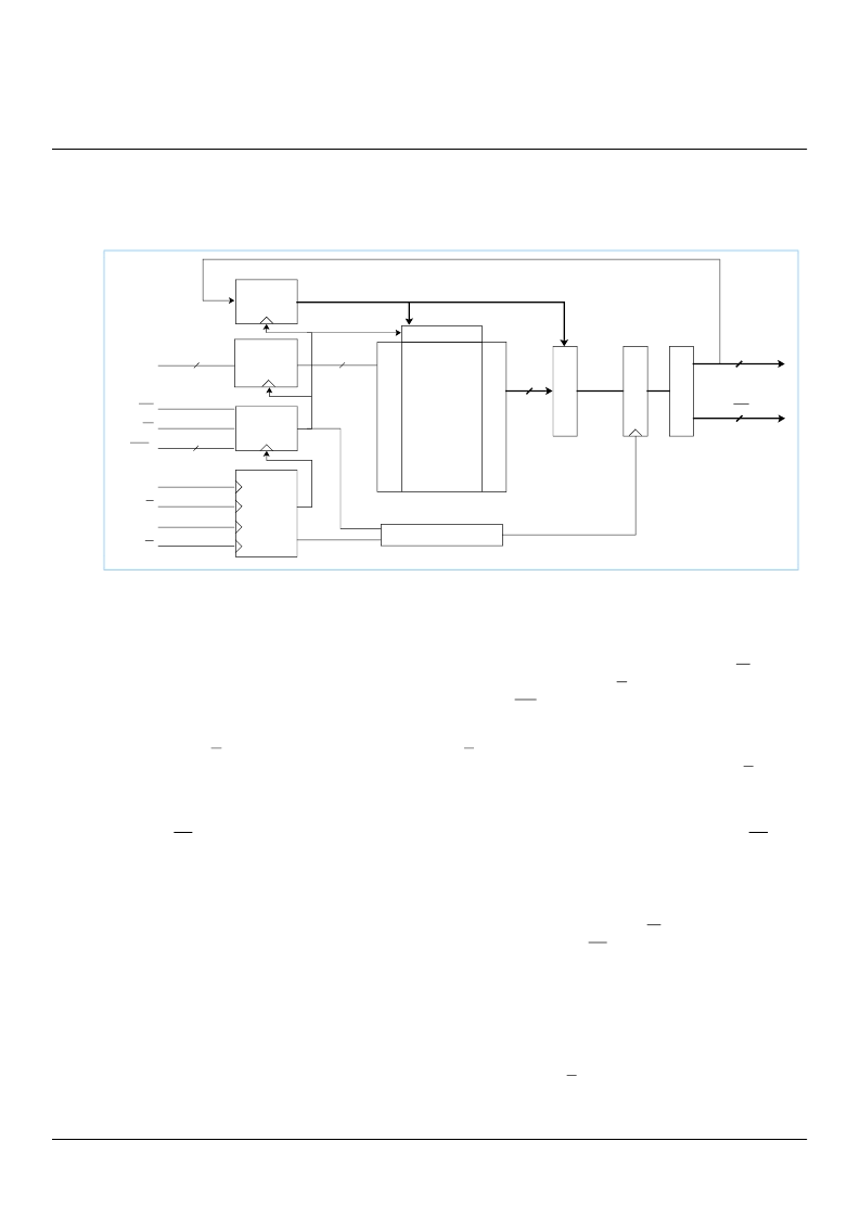
Block Diagram
1M x 36
(2M x 18)
Memory
Array
W
S
Write Driver
Select Output Control
Data
Reg
Add Reg &
Burst
Control
Control
Logic
Clock
Gen
O
O
O
36
(or 18)
72
(or 36)
36 (or 18)
DQ (Data-Out
& Data-In)
CQ, CQ
(Echo Clock Out)
Address
A0
LD
R/W
BW
x
K
K
C
C
4 (or 2)
19 (or 20)
19 (or 20)
36 (or 18)
36 (or 18)
相关PDF资料 |
PDF描述 |
|---|---|
| IS61DDB22M18 | 36 Mb (1M x 36 & 2M x 18) DDR-II (Burst of 2) CIO Synchronous SRAMs |
| IS61DDB22M18-250M3 | 36 Mb (1M x 36 & 2M x 18) DDR-II (Burst of 2) CIO Synchronous SRAMs |
| IS61DDB41M36-250M3 | 36 Mb (1M x 36 & 2M x 18) DDR-II (Burst of 4) CIO Synchronous SRAMs |
| IS61DDB42M18 | 36 Mb (1M x 36 & 2M x 18) DDR-II (Burst of 4) CIO Synchronous SRAMs |
| IS61DDB42M18-250M3 | 36 Mb (1M x 36 & 2M x 18) DDR-II (Burst of 4) CIO Synchronous SRAMs |
相关代理商/技术参数 |
参数描述 |
|---|---|
| IS61DDB21M36-250M3L | 功能描述:静态随机存取存储器 36M (1Mx36) 250MHz DDR II Sync 静态随机存取存储器 RoHS:否 制造商:Cypress Semiconductor 存储容量:16 Mbit 组织:1 M x 16 访问时间:55 ns 电源电压-最大:3.6 V 电源电压-最小:2.2 V 最大工作电流:22 uA 最大工作温度:+ 85 C 最小工作温度:- 40 C 安装风格:SMD/SMT 封装 / 箱体:TSOP-48 封装:Tray |
| IS61DDB21M36-275M3 | 功能描述:静态随机存取存储器 36M (1Mx36) 275MHz DDR II Sync 静态随机存取存储器 RoHS:否 制造商:Cypress Semiconductor 存储容量:16 Mbit 组织:1 M x 16 访问时间:55 ns 电源电压-最大:3.6 V 电源电压-最小:2.2 V 最大工作电流:22 uA 最大工作温度:+ 85 C 最小工作温度:- 40 C 安装风格:SMD/SMT 封装 / 箱体:TSOP-48 封装:Tray |
| IS61DDB21M36A-250M3L | 功能描述:静态随机存取存储器 36Mb 1Mx36 165ball DDR II Sync 静态随机存取存储器 RoHS:否 制造商:Cypress Semiconductor 存储容量:16 Mbit 组织:1 M x 16 访问时间:55 ns 电源电压-最大:3.6 V 电源电压-最小:2.2 V 最大工作电流:22 uA 最大工作温度:+ 85 C 最小工作温度:- 40 C 安装风格:SMD/SMT 封装 / 箱体:TSOP-48 封装:Tray |
| IS61DDB22M18 | 制造商:ISSI 制造商全称:Integrated Silicon Solution, Inc 功能描述:36 Mb (1M x 36 & 2M x 18) DDR-II (Burst of 2) CIO Synchronous SRAMs |
| IS61DDB22M18-250M3 | 功能描述:静态随机存取存储器 36Mb 2Mbx18 DDR II Sync 静态随机存取存储器 RoHS:否 制造商:Cypress Semiconductor 存储容量:16 Mbit 组织:1 M x 16 访问时间:55 ns 电源电压-最大:3.6 V 电源电压-最小:2.2 V 最大工作电流:22 uA 最大工作温度:+ 85 C 最小工作温度:- 40 C 安装风格:SMD/SMT 封装 / 箱体:TSOP-48 封装:Tray |
发布紧急采购,3分钟左右您将得到回复。